


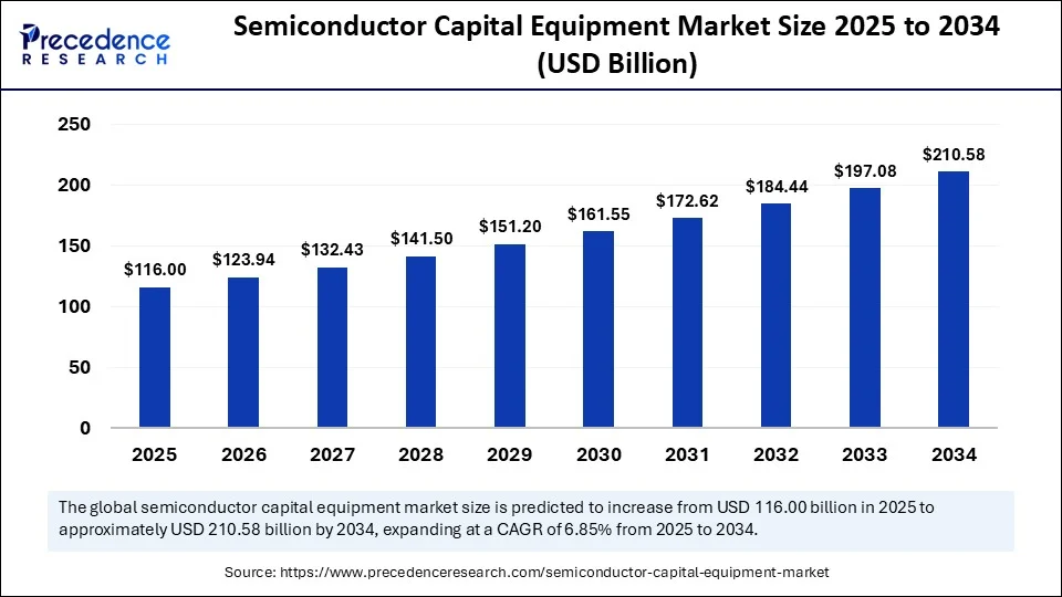
According to Precedence Research, the global semiconductor capital equipment market size is projected to reach around USD 210.58 billion by 2034 from USD 108.56 billion in 2024, with a CAGR of 6.85%.
Fueled by exponential demand in AI, 5G infrastructure, IoT, automotive electrification, and advanced packaging technologies, the semiconductor equipment market is experiencing seismic growth. Government incentives, regional reshoring policies, and the rise of advanced node manufacturing further reinforce demand across foundries and IDMs.
Semiconductor Capital Equipment Market Quick Insights
- The market was valued at USD 108.56 billion in 2024 and is estimated at USD 116.00 billion in 2025. Forecast value for 2034: USD 210.58 billion
- Compound annual growth rate: 6.85% from 2025 to 2034
- Asia Pacific held the largest share (47%) in 2024, expanding at 6.96% CAGR
- North America is expected to grow at a notable CAGR during the forecast period
- By equipment type: Front-end equipment led the market in 2024
- By application: Foundry operations segment contributed the biggest share in 2024; OSAT to see fastest future growth
Revenue Forecast Table
| Year | Market Size (USD Billion) |
|---|---|
| 2024 | 108.56 |
| 2025 | 116.00 |
| 2034 | 210.58 |
What Role Does AI Play in Transforming the Market?
Artificial intelligence is increasingly embedded across semicap infrastructure. By enabling predictive maintenance, real-time yield optimization, and automated defect detection, AI is enhancing both throughput and precision of capital equipment. This reduces unscheduled downtime and supports faster ramp-up to smaller process nodes.
AI also drives innovation in equipment design. Next-generation lithography and inspection tools now incorporate machine-learning-based analytics to adaptively adjust process parameters, improving accuracy and efficiency in sub-5nm and heterogeneous packaging lines.
Opportunities & Trends: What Questions Are Shaping the Future?
What’s driving demand for new-generation tools?
The surge in EUV lithography, 3nm and below nodes, and high-bandwidth memory packaging is pushing fabs to invest heavily in next-tier capital equipment.
How are policy shifts impacting growth?
Government initiatives like the U.S. CHIPS Act and Asia-Pacific industrial policies are accelerating fab construction and semicap purchases. Companies are also reshoring operations, boosting local tool demand.
Regional Analysis: Who’s Leading?
Asia Pacific
Dominated the market in 2024 with 47% share, totalling USD 51.02 billion, and is projected to reach USD 100.03 billion by 2034 at a CAGR of 6.96%.
Major growth stems from China, Taiwan, South Korea, and Japan, home to leading semiconductor fabs and equipment investments.
North America
Benefiting from reshoring trends and strong federal incentives, North America is forecasted to deliver notable CAGR from 2025 to 2034. Increasing in-house foundry and packaging capacities will further drive capital equipment demand.
Europe, Middle East & Africa (EMEA)
While smaller in base size, EMEA is expected to register strong growth driven by strategic autonomy initiatives, EU support for local semiconductor ecosystems, and expanding automotive chip needs.
Segmentation Highlights
By Equipment Type
Front-end equipment led in 2024, powering wafer fabrication in lithography, deposition, and etching. Back-end tools assembly, packaging, test are gaining traction due to advanced packaging demand.
By Application
The Foundry segment holds the largest share in 2024, while OSAT (Outsourced Semiconductor Assembly & Test) is expected to grow fastest during forecast due to rising need for heterogeneous integration.
By Technology Node & Wafer Size
≥ 28 nm remained dominant in 2024, but 3 nm and below tools are the fastest growing. 300 mm wafers generated majority revenue in 2024; both 300 mm and 450 mm expected to see robust growth in coming years.
By End-use Industry
Consumer electronics accounted for the largest share in 2024; automotive (especially EV and ADAS) is set for high CAGR from 2025 to 2034.
Semiconductor Capital Equipment Market Key Players
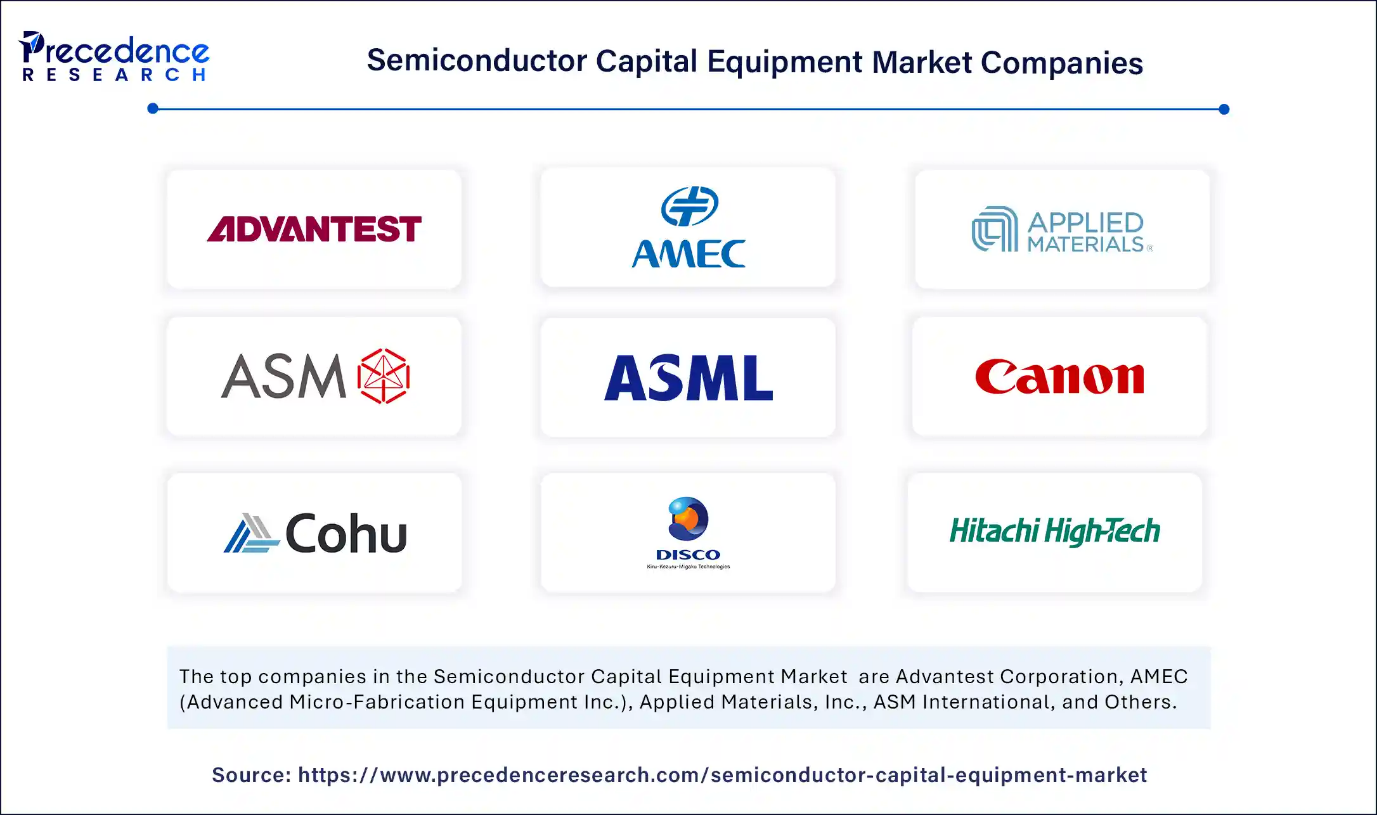
- Advantest Corporation
- AMEC (Advanced Micro-Fabrication Equipment Inc.)
- Applied Materials, Inc.
- ASM International
- ASML Holding
- Canon Inc.
- Cohu, Inc.
- DISCO Corporation
- Hitachi High-Tech Corporation
- KLA Corporation
- Lam Research Corporation
- NAURA Technology Group Co., Ltd.
- Nikon Corporation
- Nova Measuring Instruments Ltd.
- Onto Innovation Inc.
- SCREEN Holdings Co., Ltd.
- Teradyne, Inc.
- Tokyo Electron Limited
- ULVAC, Inc.
- Veeco Instruments Inc.
Breakthroughs from Key Players
Leading equipment suppliers such as ASML, Applied Materials, Lam Research, and Tokyo Electron continue to launch AI-enhanced lithography, defect inspection, and packaging tools, enabling wafer-level integrations and multi-die stacking. Their latest platforms support EUV, extreme packaging, and automated process control for next-gen fabs.
Challenges & Cost Pressures
- Sky-high CapEx Needs: Modern tools like EUV scanners and high-speed testers cost hundreds of millions per installation.
- Supply Chain Risks: Geopolitical tensions and export control measures (e.g. US restrictions on China) disrupt equipment flows and raise input costs.
- Talent Gap: Engineers skilled in photonics, lithography, and AI-enabled process engineering remain scarce globally.
Case Study: AI-Driven Yield Gains in PackagingA leading foundry deployed an AI-empowered defect inspection suite across its advanced packaging line. Yield improved by 10-15%, defect detection sped up by over 50%, and overall scrap rates declined demonstrating how AI-guided tools deliver measurable ROI in high-complexity process environments.


 combined with superior switching performance")


