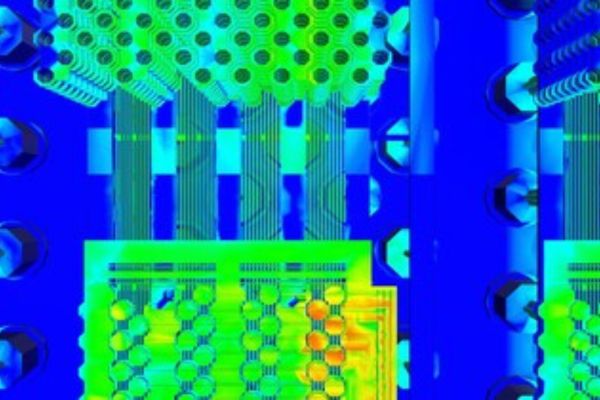
Ansys , announced thermal and multiphysics signoff tool certifications for designs manufactured with Intel 18A process technology. These certifications help ensure functionality and reliability of advanced semiconductor systems for the most demanding applications including AI chips, graphic processing units (GPUs), and high-performance computing (HPC) products. Intel Foundry and Ansys have also enabled a comprehensive multiphysics signoff analysis flow for Intel Foundry’s EMIB technology used for creating multi-die 3D integrated circuit (3D-IC) systems.
Recognized as industry-leading solutions, RedHawk-SC and Totem deliver speed, accuracy, and capacity to analyze the power integrity and reliability of Intel 18A RibbonFET Gate-all-around (GAA) transistors with PowerVia backside power delivery. For scalable electromagnetic analysis, Ansys is introducing HFSS-IC Pro, a new addition to the HFSS-IC product family. HFSS-IC Pro is certified for modeling on-chip electromagnetic integrity in radio frequency chips, WiFi, 5G/6G, and other telecommunication applications made with the Intel 18A process node.
EMIB facilitates 3D-IC for high-performance microprocessors, heterogeneous integrated systems, and more, enhancing the performance and integration of advanced computing systems by seamlessly connecting diverse chip types. The flow includes thermal reliability analysis with RedHawk-SC Electrothermal. Ansys and Intel Foundry are also extending the collaboration to cover next-generation EMIB-T technology that will add through-silicon vias (TSVs) to EMIB. The EMIB-T flow is expanded to include HFSS-IC Pro and SIwave for signal integrity analysis and RedHawk-SC and Totem for power integrity analysis.
The qualification process for RedHawk-SC, Totem, and HFSS-IC Pro is currently in progress for the Intel 18A high-performance process node (Intel 18A-P). Customers have the option to request the latest Intel PDK to begin early design work and IP development. These solutions are part of the Intel 14A-E process definition and Design Technology Co-Optimization (DTCO).
In addition, Ansys is joining the Intel Foundry Chiplet Alliance, part of the Intel Foundry Accelerator Alliance, to help develop a secure ecosystem for designing and manufacturing interoperable chiplets.
“Our approach to multi-die assembly is changing the way the industry thinks about stacking chips and designing for efficiency,” said Suk Lee, vice president & general manager, Ecosystem Technology Office at Intel Foundry. “Ansys tools are critical in this process because they help our mutual customers validate their designs with extreme accuracy — saving them costs that may not otherwise be recoverable. Furthermore, we are looking forward to Ansys’ participation in the Intel Foundry Chiplet Alliance, which is critical to advancing chiplet technology.”
“Ansys’ suite of multiphysics simulation tools instill confidence in our customers, ensuring their semiconductor systems achieve the highest levels of thermal, signal, power, and mechanical integrity,” said John Lee, vice president and general manager of the electronics, semiconductor, and optics business unit at Ansys. “While customers may adopt various methods for chip design, the need for precise tools and solutions to ensure reliability remains constant — this is where Ansys excels. By joining the Intel Foundry Chiplet Alliance and deepening our collaboration with Intel Foundry, Ansys is delivering on its commitment to providing open-source and interoperable technology in pursuit of engineering excellence.”


