


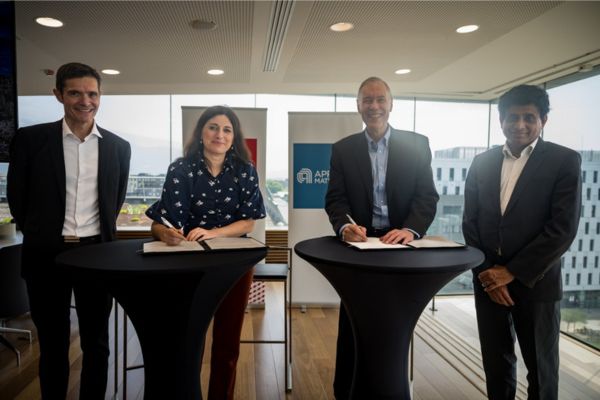
Applied Materials, and CEA-Leti announced the next phase of their longstanding collaboration to accelerate innovation in specialty semiconductors. Through an expansion of their joint lab, the organizations plan to develop materials engineering solutions to address emerging infrastructure challenges in AI data centers.
The joint lab is focused on device innovations for chipmakers serving ICAPS markets (IoT, Communications, Automotive, Power and Sensors). These specialty chips are used in a wide range of applications – from industrial automation to electric vehicles – and they play a critical role managing data and power distribution within data centers. Growing resource demands in AI infrastructure have highlighted the need for a new wave of innovation in ICAPS chips to enable more energy-efficient computing.
Under the new agreement, Applied and CEA-Leti will expand the lab with new equipment and capabilities that move beyond individual process steps to include full-flow development of specialty devices. Additionally, the lab will be equipped with state-of-the-art advanced packaging tools to support heterogeneous integration of chips across different wafer types and process nodes – enabling entirely new classes of specialty devices for a range of next-generation applications.
The joint facility features several Applied Materials wafer processing systems together with CEA-Leti’s world-class capabilities for evaluating performance of new materials and device validation. The upgraded lab will strengthen the chipmaking ecosystem in France by further expanding the technology hub in Grenoble, a leading site for collaborative innovation across government, academia and industry. The lab also marks an extension of Applied’s global EPIC Platform, a new high-velocity innovation model designed to accelerate commercialization of new chip technologies. Applied and CEA-Leti will be able to leverage the R&D work taking place across Applied’s global innovation centers to drive progress in specialty semiconductor technologies.
“Applied Materials and CEA-Leti have a long history of successful collaboration, and we are excited to strengthen our capabilities for accelerating innovation and commercialization of next-generation specialty chips,” said Aninda Moitra, corporate vice president and general manager of Applied Materials’ ICAPS business. “Our combined expertise will help foster breakthroughs and push the boundaries of semiconductor innovation, contributing to sustainable advancements in a range of critical applications for the AI era.”
Sébastian Dauvé, CEO of CEA-Leti, said the first phase of the expanded collaboration laid important groundwork for addressing materials-engineering challenges of specialty semiconductor devices.
“Building on this momentum, the joint lab’s new focus on energy-efficient solutions for AI data-center infrastructure reflects our shared commitment to making technological progress that meets both industrial and societal needs. The extended partnership also leverages our complementary strengths to accelerate innovation at the system level, while supporting sustainable growth in France’s semiconductor ecosystem,” he said.


 combined with superior switching performance")


