


A recently concluded 42-month EU project, ELENA, announced the development of the first-ever, European-made lithium niobate on insulator (LNOI) substrates for photonic integrated circuits (PICs)—a breakthrough that establishes a fully European supply chain for thin-film lithium niobate (TFLN) technology.
TFLN is a breakthrough material platform enabling high-performance PICs through its thin-film structure, offering unique electro-optic, nonlinear optical, and acousto-optic properties. The advent of LNOI wafers allows micromachining of LN with high precision, integrating multiple optical functions within a footprint smaller than a fingertip. These attributes make LNOI particularly attractive for high-speed, low-power optical communications and quantum systems.
Until now, the LNOI ecosystem has been constrained by a limited supply chain reliant on a single commercial supplier outside the EU—and the absence of a commercial foundry capable of producing TFLN photonic chips at scale. The ELENA project directly addressed these critical gaps by establishing Europe’s first commercial LNOI wafer supply and laying the groundwork for a TFLN photonic chip foundry.
The €5 million initiative united 10 partners across the PIC value chain—from substrate innovation and photonic design to manufacturing, testing, and packaging. Key outcomes include the first process design kit (PDK) for the LNOI platform and advances in foundry-compatible processes to transition TFLN technology from research to commercial production. This effort significantly enhances European sovereignty in a strategically vital segment of the semiconductor supply chain.
Spinout Launched to Produce TFLN Photonic Chips on 150mm Optical Grade Wafers
A cornerstone of the project is the creation of Europe’s first open-access LNOI photonic chip foundry at the Swiss Center for Electronics and Microtechnology’s (CSEM) certified cleanroom facility in Neuchâtel, Switzerland. There, TFLN chips will be produced on 150 mm optical-grade LNOI wafers at industrial scale. As a result, CSEM, which coordinated the project, has launched CCRAFT, a dedicated spinout to scale up production.
“The spinout foundry is uniquely positioned at the core of the TFLN value chain, because it delivers production-grade service, a rare block in the supply chain,” said Hamed Sattari, ELENA’s project manager and CEO of CCRAFT. “CCRAFT’s roadmap includes expanding capacity to deliver millions of TFLN chips annually, firmly positioning Europe as a global leader in photonic-chip manufacturing.”
The availability of a production-grade photonic chip foundry, combined with project members CEA-Leti and SOITEC’s plans to commercialize LNOI wafers, also supports Europe’s ability to manufacture the next generation of photonic chips across a broad range of markets and industries.
Meeting Diverse Market Needs with Demonstrator Prototypes
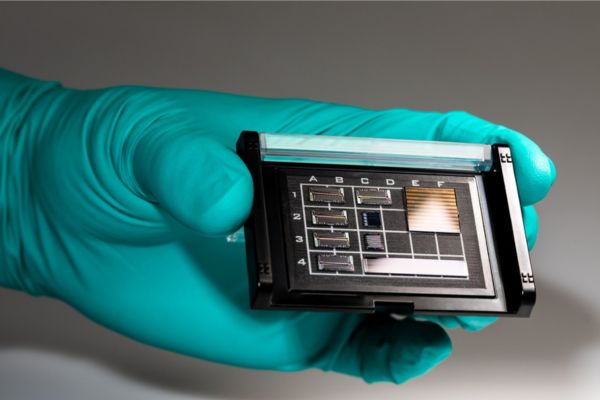
To validate the platform, ELENA produced four demonstrator PICs targeting high-impact sectors:
- Quantum: ion trapping, optical clocks, entangled photon generation,
- Telecom: >400 Gbit/s modulators, DWDM, CMOS-compatible transceivers,
- Space: lightweight, low-power PICs for satellite communications, and
- LIDAR/Sensing: compact, efficient systems for automotive, medical, and environmental monitoring.
As demand surges for faster, energy-efficient electro-optic chips across AI, data centers, and telecommunications, ELENA’s achievement firmly positions the EU at the forefront of global photonics innovation.
The partners, which include leading European research institutes, large industrial companies and SMEs (short names in brackets), are:
1) Swiss Center for Electronics and Microtechnology (CSEM), Switzerland;
2) CEA-Leti (Leti), France;
3) SOITEC SA (Soitec), France;
4) VPIphotonics GmbH (VPI), Germany;
5) Eidgenössische Technische Hochschule Zürich (ETHZ), Switzerland;
6) Vanguard Automation GmbH (VA), Germany;
7) Thales SA (THALES), France;
8) III-V LAB (III-V LAB), France;
9) Rosenberger Hochfrequenztechnik GmbH & Co. KG (ROS), Germany; and
10) L-up SAS (LUP), France.


 combined with superior switching performance")


