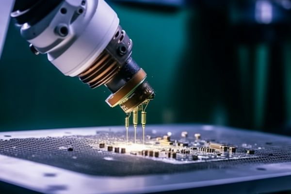
The semiconductor industry is continuously innovating to meet the demands for higher performance, greater storage capacities, and enhanced energy efficiency. Among these advancements, 3D NAND technology stands out as a transformative development in memory storage. 3D NAND and other emerging trends are poised to shape the future of semiconductor manufacturing. As per the Consegic Business Intelligence analysis, 3D Semiconductor Packaging Market size is estimated to reach over USD 35.30 Billion by 2031 from a value of USD 9.43 Billion in 2022 and is projected to grow by USD 10.73 Billion in 2023, growing at a CAGR of 16.1% from 2023 to 2031.
3D NAND Technology
3D NAND, also known as vertical NAND, stacks memory cells in multiple layers to increase storage density and reduce the cost per bit. This technology overcomes the limitations of planar NAND, where memory cells are arranged horizontally on a silicon wafer. 3D NAND significantly boosts storage capacity by stacking memory cells vertically. Current advancements have seen companies like Samsung reaching up to 176 layers, and SK Hynix and Micron developing similar high-layer architectures, leading to higher capacity SSDs in smaller form factors.
The vertical structure of 3D NAND reduces the distance data must travel, resulting in enhanced read and write speeds. This translates to faster performance for applications ranging from consumer electronics to enterprise data centers. The increased parallelism in 3D NAND architecture also contributes to better performance. 3D NAND technology offers improved durability compared to planar NAND. The larger cells and advanced error correction mechanisms extend the lifespan of memory devices. Manufacturers like Toshiba and Western Digital have incorporated these features to enhance product longevity.
By stacking cells vertically, 3D NAND reduces power consumption, making it ideal for mobile devices and other applications where energy efficiency is crucial. This reduction in power usage helps prolong battery life in portable electronics and reduces overall energy costs in data centers.
Emerging Trends in Semiconductor Manufacturing
3D XPoint Technology
3D XPoint, co-developed by Intel and Micron, represents a new class of non-volatile memory that bridges the performance gap between DRAM and NAND flash. This technology offers faster data access speeds and greater endurance than traditional NAND, making it suitable for a wide range of high-performance applications. 3D XPoint provides significantly faster read and write speeds compared to NAND flash, up to 1,000 times faster in some cases. This makes it ideal for real-time data processing applications and high-performance computing tasks. The technology can endure more write cycles than NAND, enhancing the lifespan of storage devices. This makes 3D XPoint particularly valuable for applications requiring frequent data writes, such as caching and storage for AI workloads.
Extreme Ultraviolet Lithography (EUV)
EUV lithography uses extreme ultraviolet wavelengths to etch finer patterns on silicon wafers, enabling the production of smaller and more powerful semiconductor devices. EUV is critical for continuing Moore’s Law as traditional photolithography approaches its physical limits. Companies like ASML are leading the way in EUV technology, providing essential tools for the latest chip manufacturing processes.
Multi-Patterning
Multi-patterning techniques, such as self-aligned double patterning (SADP) and self-aligned quadruple patterning (SAQP), enable the creation of intricate semiconductor patterns necessary for producing smaller nodes like 5nm and below. These techniques allow for the continued miniaturization of semiconductor devices, which is essential for improving performance and efficiency.
Conclusion
The future of semiconductor manufacturing is marked by groundbreaking innovations such as 3D NAND, advanced lithography, heterogeneous integration, and emerging computing paradigms like quantum and neuromorphic computing. These advancements promise higher performance, greater efficiency, and new capabilities, driving the next wave of technological progress across various industries. As these technologies mature, they will redefine the landscape of semiconductor manufacturing, paving the way for future innovations that will continue to push the boundaries of what is possible.


