Introduction
Smaller and more efficient power converters is the trend of the last decades. And it is expected to remain so in the future. This is achieved using new topologies, new materials and new integration processes. New materials integration was the focus of the European Union’s Horizon 2020 Project as it funded the GaNonCMOS project. The project was aimed at the dense integration of GaN and Si at different levels (PCB, stack and chip), developing new soft magnetic materials suitable for high switching frequencies and PCB embedding. Unlike the “mainstream” use of GaN materials in the 650V range, the project’s area of interest was sub 100V DC/DC conversion–low power PoL converters for server applications as well as the automotive and aerospace industries. Eleven industry leaders and research institutes from Austria, Belgium, Germany, Netherlands and Ireland participated in this project. The RECOM group participated in the development of these new technologies, following the company’s goal to bring innovative, integrated (3DPP) and more reliable solutions in the field of power conversion.
Embedding
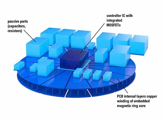
One of the focus areas of the project was embedding components into the PCB. With this technique, it is possible to hide one or more components in the PCB core. The main limitation of embedding is the thickness of the component and its behaviour under various environmental conditions. The embeddable component could be an IC, switch or passive, depending on the goals of the design. By using thick copper planes connected to the leads of the embedded component, a well-defined thermal path can be created. The IC and MOSFET bodies can be placed very close to each other, reducing the parasitic inductance and enabling a higher switching speed. Small passives such as resistors and capacitors can be embedded in the same cavity, while only the larger components such as magnetics, input or output capacitors stay outside. The capacitors are then especially less stressed by the heat from the switches or IC by means of the FR4 material. The whole layout is then made more complex due to its 3D structure, but it may have the advantage of smaller switching and control loops. Other important advantages include the smaller solution area and the protection of the design against reverse engineering.
Another approach is to focus on reducing the height of the PCB. For example, in a buck converter design, the inductor is typically the tallest component. If a very flat solution is needed, it might be impossible to find a suitable low-profile inductor. In this project, the idea of embedding magnetics was realized. But how could one embed the inductor with specific parameters, for which the chip size equivalents are a way too big for embedding? This hurdle was answered using magnetic sheet materials. Very thin (100–200 μm) materials with certain magnetic characteristics can be cut into different shapes and placed on the PCB. The PCB routing formed a winding structure. Such an inductor can possess a relatively large area compared to the chip inductor, which is compact but tall. Several demonstrators with this technology have been built. The ideal solution for reduction of space is for the inductor area to be around the same size as the other small components placed on the PCB (see Figure 1). The depicted illustration uses a ring core shape with the windings in the inner layer, creating a toroidal inductor (see Figure 2). Other shapes and other winding structures are also possible, depending on the available space, necessary coupling, current capability, etc. Figure 3 depicts a simple 1:1 transformer design based on the same ring core shape of the magnetic material. The advantage of having the transformer embedded is an increased pollution degree and decreased creepage and clearance requirements. It is obvious that the area needed to meet higher inductance values and higher current increases. Even though the embedding process of magnetic sheets has been verified on larger areas (10×10 cm), too, its main sweet spot is mainly in lower current range applications – up to 2A. There are parameters such as the number of windings that increase the DCR of the final inductor and decrease the overall efficiency.
Materials and reliability
Within the project, more than 10 different sheet materials were tested to determine their suitability for embedding. Much like chip inductor materials, sheet materials differ, too. The sheets are embedded under high pressure and then they are encapsulated in the PCB. Long-term reliability tests based on the automotive standard (AEC Q200) with large number of samples were performed to evaluate the stability of the electrical parameters and mechanical consistency. Examples of the tests include the following: temperature cycling (2000 cycles); temperature humidity bias (1000 hours at 85°C, 85% RH); high temperature storage (1000 hours at 125°C); low temperature storage (1000 hours at -55°C); highly accelerated stress test (96 hours at 130°C, 85% RH). Only a few materials passed these tests without a shift in the parameters or delamination within the PCB. This knowledge helps to avoid main risks in designing with this technology, as some materials crack during the embedding process.
The most of these sheet materials are suitable for switching frequencies between 1MHz to 5MHz. Other than the testing of magnetic sheet materials, the project also focused on developing new magnetic materials suitable for switching frequencies around 20MHz. Several trials lead to a new compound that was successfully embedded, too.
Chip-level integration
As the name of the project indicates, one of the project goals was to integrate a GaN device (the switch) with the CMOS driver. Both GaN and Si devices have been self-developed and manufactured within the project in several iterations in order to meet the electrical and physical requirements of the integration process. The newly developed process is called direct wafer bonding (IBM) and allows to bond two wafers before dicing. This complex process is still in the trial stage, but when the anticipated obstacles are overcome, it will be another milestone in chip integration as two different semiconductor materials in one device combines the best of both worlds. Practically, no parasitic inductance between the driver and the switch would allow extremely high switching frequency in the range of hundreds of MHz. This results in minimal size requirements on the passives (magnetics and capacitors), leading to extreme reduction in the volume for power conversion.


GaNonCMOS members: Katholieke Univeriteit Leuven, University College Cork – National University of Ireland (Tyndall – UCC), Fraunhofer Gesellschaft zur Förderung der Angewandten Forschung E.V, IHP GmbH – Innovations for High Performance Microelectronics/Leibniz-Institut für Innovative Mikroelektronik GmbH, EpiGan NV, IBM Research GmbH, AT&S Austria Technologie & Systemtechnik Aktiengesellschaft AG, RECOM Engineering GmbH & CO KG, NXP Semiconductors Netherlands BV, X-FAB Semiconductor Foundries AG, PNO Innovation NV
About the author
Stanislav Suchovsky, R&D Engineer at RECOM, He graduated from Slovak Technical University in 2002 with a degree in Electrical Engineering and a thesis on test and measurement systems. He then worked for 14 years, designing AC/DC and DC/DC power supplies for aerospace applications. His focus at RECOM is DC/DC power modules and new technologies.


