


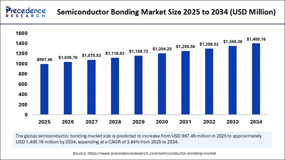
The global semiconductor bonding market will rise from USD 997.46 million in 2025 to USD 1,400.16 million by 2034, expanding at a compound annual growth rate (CAGR) of 3.84 %. The market measured USD 960.57 million in 2024 and is riding the wave of miniaturized electronics, 3D chip stacking and high-performance computing. As chipmakers intensify adoption of hybrid bonding and 3D integration to build densely packed devices, semiconductor bonding tools are becoming indispensable for smartphones, electric vehicles, advanced driver-assistance systems (ADAS), data-centre processors and the artificial-intelligence (AI) revolution.
“Semiconductor bonding is the unsung hero of the 3D chip revolution,” says Dr Anika Prakash, Principal Consultant at Precedence Research. “Every generational leap in AI processors or autonomous vehicles requires bonding technologies that can align and interconnect multi-die packages with sub-micron accuracy. Our latest study shows that companies investing in hybrid bonding and thermocompression equipment today will become tomorrow’s leaders in AI, automotive and consumer electronics.”
Semiconductor Bonding Market Insights
| Attribute | Highlights |
| Market Size in 2024 | USD 960.57 Million |
| Market Size in 2025 | USD 997.46 Million |
| Market Size By 2034 | USD 1,400.16 Million |
| CAGR (2025-2034) | 3.84% |
| Leading Region (2024) | Asia Pacific, commanding 65 % share due to its extensive packaging capacity |
| Fastest-Growing Region | North America is set to grow at the highest CAGR thanks to on-shore investments and policy support |
| Top Bonding Technology (2024) | Wire bonding held 55 % share; flip-chip bonding will register fastest growth |
| Top Bonding Material (2024) | Gold wire/ball dominated with 40 % share; copper wire/pillars will grow fastest |
| Key End User (2024) | Outsourced assembly & test (OSATs) captured 50 % share |
| Recent Breakthroughs | Applied Materials & BESI co-develop hybrid bonding system (Apr 2025); BESI raised revenue targets amid AI-driven demand (Jun 2025);LG Electronics developed in-house hybrid bonding machine for high-bandwidth memory (Jul 2025) |
Detailed Market Snapshot
The semiconductor bonding market serves as the backbone of backend packaging, providing die bonding, flip-chip bonding, wafer-to-wafer bonding and hybrid bonding equipment. It enables vertical stacking of chips in 3D integrated circuits (ICs), system-in-package (SiP) and chiplets for AI and high-performance computing. The report identifies several core trends:
- Miniaturization & 3D packaging drive demand. Advanced bonding methods facilitate vertical chip stacking to meet space and performance requirements of smartphones, wearable electronics and 3D ICs.
- Consumer electronics & automotive growth. The proliferation of smartphones, wearables, electric vehicles and ADAS systems fuels adoption of 3D packaging and bonding technologies.
- High-performance chips for AI, 5G and IoT. The surge in AI processors and 5G infrastructure necessitates faster, low-power chips requiring precise bonding and hybrid wafer bonding.
- Advances in bonding equipment. Innovations such as hybrid bonding and thermocompression bonding enhance process efficiency, improving throughput and yield.
- Rise of semiconductor foundries & packaging houses. Investments in back-end manufacturing facilities support global supply resilience.
Regional Highlights
Asia‑Pacific’s Manufacturing Muscle Enough to Drive the Semiconductor Bonding Boom?
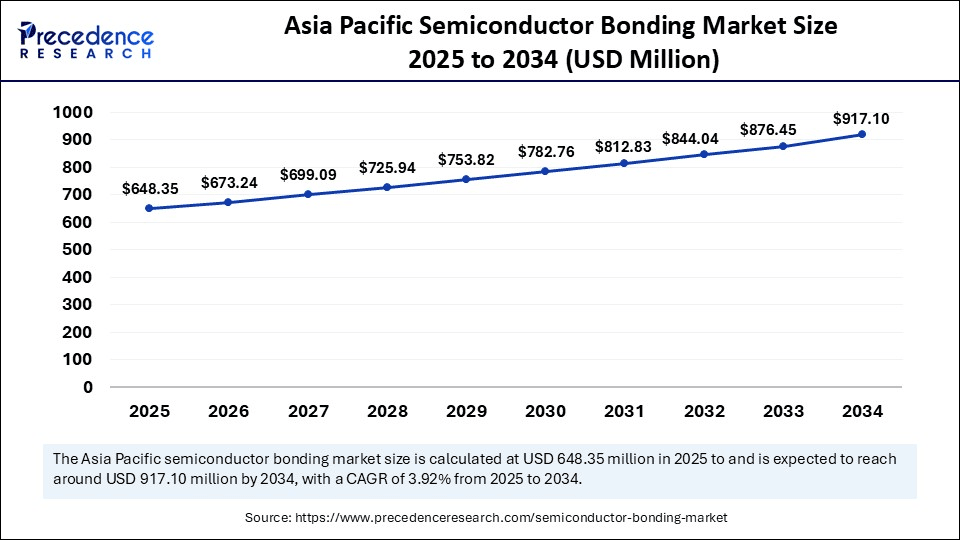
Asia Pacific semiconductor bonding market size was USD 624.37 million in 2024 and is expected to expand around USD 917.10 million by 2034, at a CAGR of 3.92% from 2025 to 2034.
- Asia Pacific commanded 65 % of global revenue in 2024. China, Taiwan, South Korea and Japan host mega-foundries and packaging plants, benefiting from skilled labour, cost advantages and comprehensive supply chains. Government incentives and a strong ecosystem sustain its leadership.
- North America will deliver the fastest CAGR, supported by on-shoring incentives, government funding for advanced packaging and strategic sectors (AI, aerospace & defence). Investments in domestic packaging capacity and large-scale chip initiatives underpin growth.
- Europe and Latin America are adopting bonding solutions to bolster automotive and industrial electronics manufacturing. Middle East & Africa remain nascent but show potential due to investments in smart-cities and renewable energy devices.
Segment Insights
- Bonding Technology: Wire bonding remains dominant due to its cost-effectiveness and broad compatibility. However, flip-chip bonding and hybrid bonding exhibit the fastest growth as they enable high-density interconnects, better electrical performance and smaller form factors.
- Bonding Material: Gold wire/ball is prized for conductivity and reliability in high-reliability sectors like aerospace and medical devices. Copper wire/pillars are gaining traction as an economical alternative with superior conductivity, especially in smartphones and high-volume consumer electronics.
- Packaging Type: Plastic dual-in-line & QFP packages dominated 2024 due to widespread use in microcontrollers and general-purpose chips. Ball grid array (BGA) & flip-chip packages are growing quickly for AI processors, networking gear and high-performance smartphones.
- End User: OSATs captured half of the market share, offering scalable, cost-effective bonding services. Integrated device manufacturers (IDMs) are investing heavily in in-house packaging lines to improve performance and reduce time-to-market.
- Equipment vs Materials: Bonding equipment generated 60 % share due to high capital investment and process criticality. Materials & consumables (wires, bumps, adhesives) will grow faster, driven by frequent replacements and the need for low-resistance, thermally stable materials.
Market Opportunities – Where Will the Bonding Boom Come From?
1. Electric Vehicles & Automotive Electronics: As automakers transition to electric, connected and autonomous vehicles, demand for high-reliability chips and robust bonding methods will soar. Semiconductor bonding techniques must withstand harsh thermal and mechanical conditions in EVs, battery management systems and ADAS.
2. Hybrid & Heterogeneous Integration: The shift toward chiplet-based designs and heterogeneous integration offers huge opportunities for bonding providers. Advanced bonding processes enable sub-micron alignment and ultra-low interconnect pitch required for hybrid bonding and die-to-wafer bonding.
3. AI and High-Performance Computing: AI accelerators and data-center processors rely on 3D stacked memory and compute dies. (system-on-integrated-chip) roadmap illustrates the adoption of hybrid wafer bonding to stack logic devices with bond pitches shrinking from 9 μm to 3 μm by 2027. The improved bandwidth density enables ultra-dense processor designs needed for AI and HPC workloads.
Recent Developments & Competitive Landscape
- Applied Materials & BESI co-development: In April 2025, Applied Materials partnered with BE Semiconductor Industries (BESI) to create an integrated hybrid bonding system tailored for next-generation packaging. This collaboration aims to deliver sub-5 μm alignment accuracy and high-throughput production.
- BESI raises revenue targets: In June 2025, BESI increased its long-term revenue targets to €1.5–1.9 billion, citing surging demand for its hybrid bonding tools driven by AI and data-centre applications.
- LG Electronics’ in-house hybrid bonding machine: In July 2025, LG Electronics’ Production Technology Research Institute announced the development of an in-house hybrid bonding machine for high-bandwidth memory applications.
- TSMC’s SoIC progress: TSMC’s roadmap shows its SoIC-X hybrid bonding technology will reduce bond pitches from 9 μm to 3 μm by 2027, enabling stacking of A16 and N2 dies and dramatically increasing bandwidth density. The SoIC-P process, to be offered in 2025, targets cost-conscious applications with 25 μm bond pitches.
Semiconductor Bonding Market Major Companies
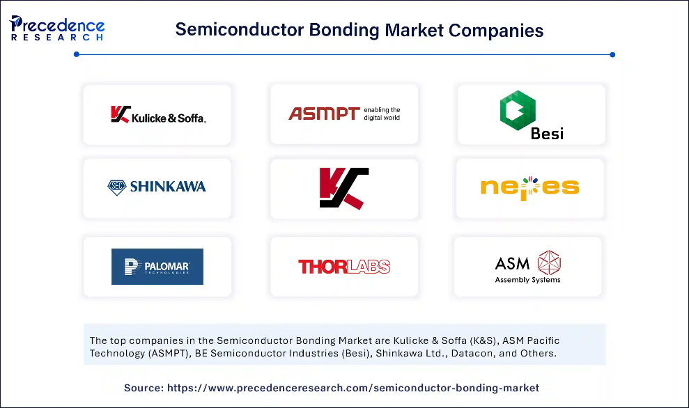
- Kulicke & Soffa (K&S)
- ASM Pacific Technology (ASMPT)
- BE Semiconductor Industries (Besi)
- Shinkawa Ltd.
- Datacon
- Kulicke & Soffa’s Palomar division
- Kulicke & Soffa’s CMG division
- Nepes Corp.
- Palomar Technologies
- ThorLabs (formerly Applied Materials Assembly)
- ASM Assembly Systems
- Datacon Technology
- Europlacer
- F&K Delvotec
- SUSS MicroTec
- Tokyo Seimitsu
- Panasonic Factory Solutions
- Finetech (Kulicke & Soffa)
- Starrag Group (Jenaer)
- Intel & TSMC
Challenges & Cost Pressures
- Process complexity: Advanced bonding techniques (hybrid, thermocompression) require precise control of alignment, temperature and pressure. Even minor deviations lead to defects and yield losses.
- Supply-chain disruptions: Geopolitical tensions and pandemic-related logistics issues can disrupt the supply of bonding materials such as copper pillars and adhesives.
- Capital intensity: High equipment costs and the need for skilled operators deter smaller players from adopting next-generation bonding technologies.


 combined with superior switching performance")


