


Objective
In this laboratory, we examine pulse width modulation and its usage within a variety of applications.
Pulse width modulation (PWM) is a method for encoding an analog signal into a single digital bit. A PWM signal consists of two main components that define its behavior: a duty cycle and a frequency.
It is used in the transmission of information by encoding a message into a pulsing signal, for power control of electronic devices such as motors, and as the principal algorithm for photovoltaic solar battery chargers.
The duty cycle describes the amount of time the signal is in a high (on) state as a percentage of the total time it takes to complete one cycle (Figure 1).
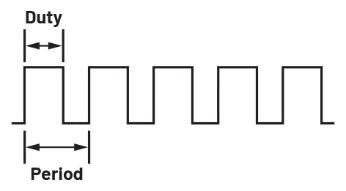
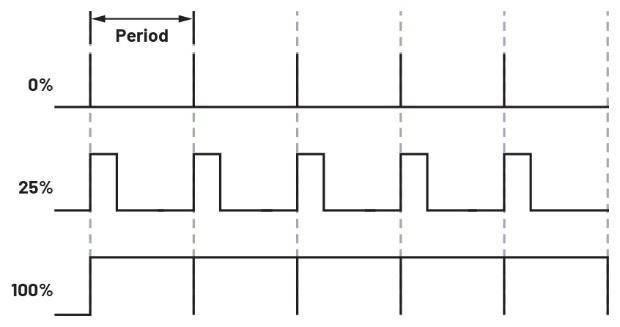
Figure 2 shows pulse trains at 0%, 25%, and 100% duty cycle.
The frequency determines how fast the PWM completes a cycle, and therefore how fast it switches between high and low states.
By varying a digital signal off and on at a fast enough rate, and with a certain duty cycle, the output will appear to behave like a constant voltage analog signal when providing power to devices that respond much slower than the PWM frequency, such as audio speakers, electric motors, and solenoid actuators.
Materials
- ADALM2000 Active Learning Module
- Solderless breadboard and jumper wire kit
- One OP97 operational amplifier
- One 1 kΩ resistor
- One 10 kΩ potentiometer
Pulse Width Modulation—Principle of Operation
PWM is a technique used to generate low frequency output signals from high frequency pulses. Rapidly switching the output voltage of an inverter leg between the upper and lower DC rail voltages, the low frequency output can be thought of as the average voltage over a switching period.
Besides that, there are several other ways of generating pulse width modulated signals, including analog techniques, sigma-delta modulation, and direct digital synthesis.
One of the simplest methods of generating a PWM signal is to compare two control signals: a carrier signal and a modulation signal. This is known as carrier-based PWM. The carrier signal is a high frequency (switching frequency) triangular waveform. The modulation signal can be any shape.
Using this approach, the output waveform can be a PWM representation of any desired waveform shape. With machines, sinusoidal and trapezoidal waveform shapes are among the most common.
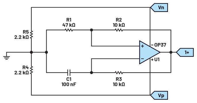
Consider the circuit in Figure 3.
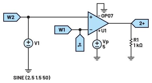
Following the description of the PWM principle, we use the negative input of the operational amplifier for the carrier, with the positive input for the modulation signal. Thus, a higher modulation signal will result in an output that is at a high level for a greater fraction of the PWM period.
Hardware Setup
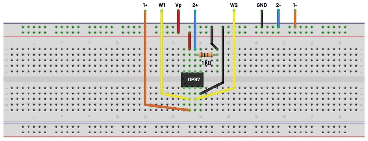
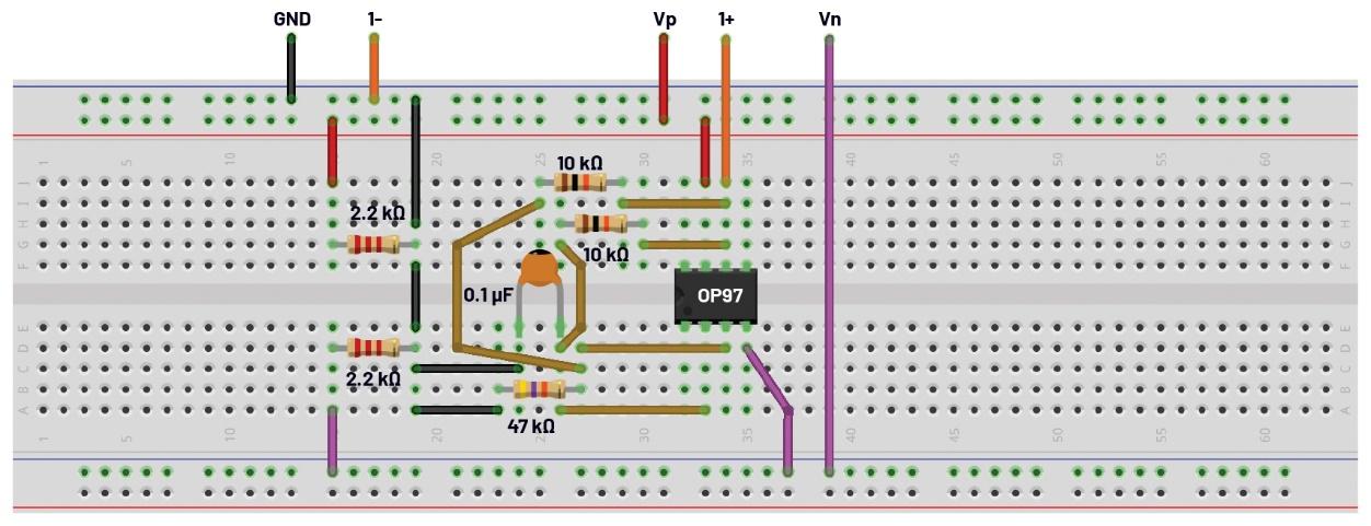
Build the breadboard circuit for PWM (Figure 4).
Procedure
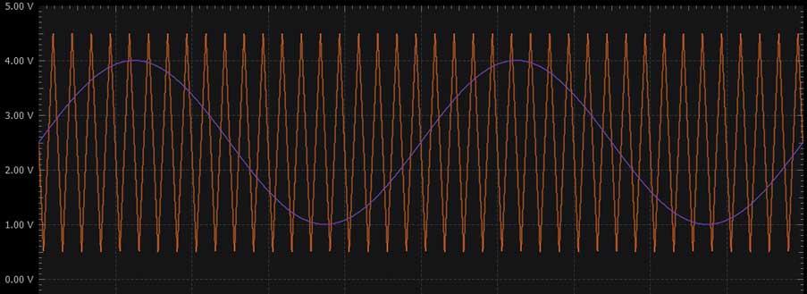
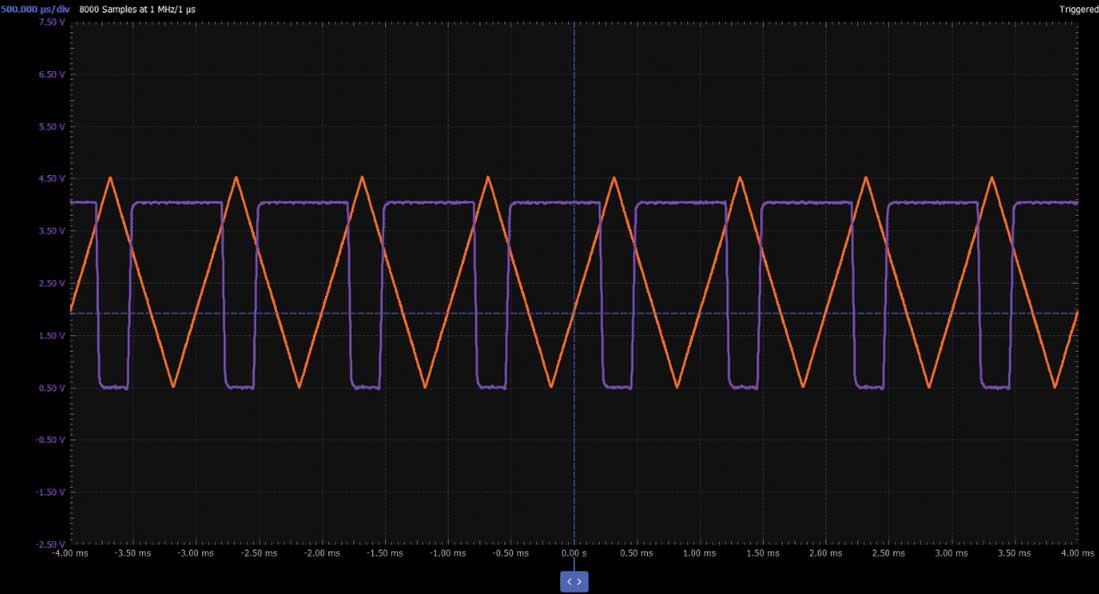
Use the first waveform generator as the carrier signal providing a 4 V amplitude peak-to-peak, 2.5 V offset, 1 kHz triangle wave excitation to the circuit. Use the second waveform generator as the modulation signal with a 3 V amplitude peak-to-peak, 2.5 V offset, 50 Hz sine wave.
Supply the op amp with +5 V from the power supply. Configure the scope so that the input signal is displayed on Channel 1 and the output signal is displayed on Channel 2.
Figure 5 shows the two signal generator channels containing the two input signals (orange, carrier signal; purple, modulation signal).
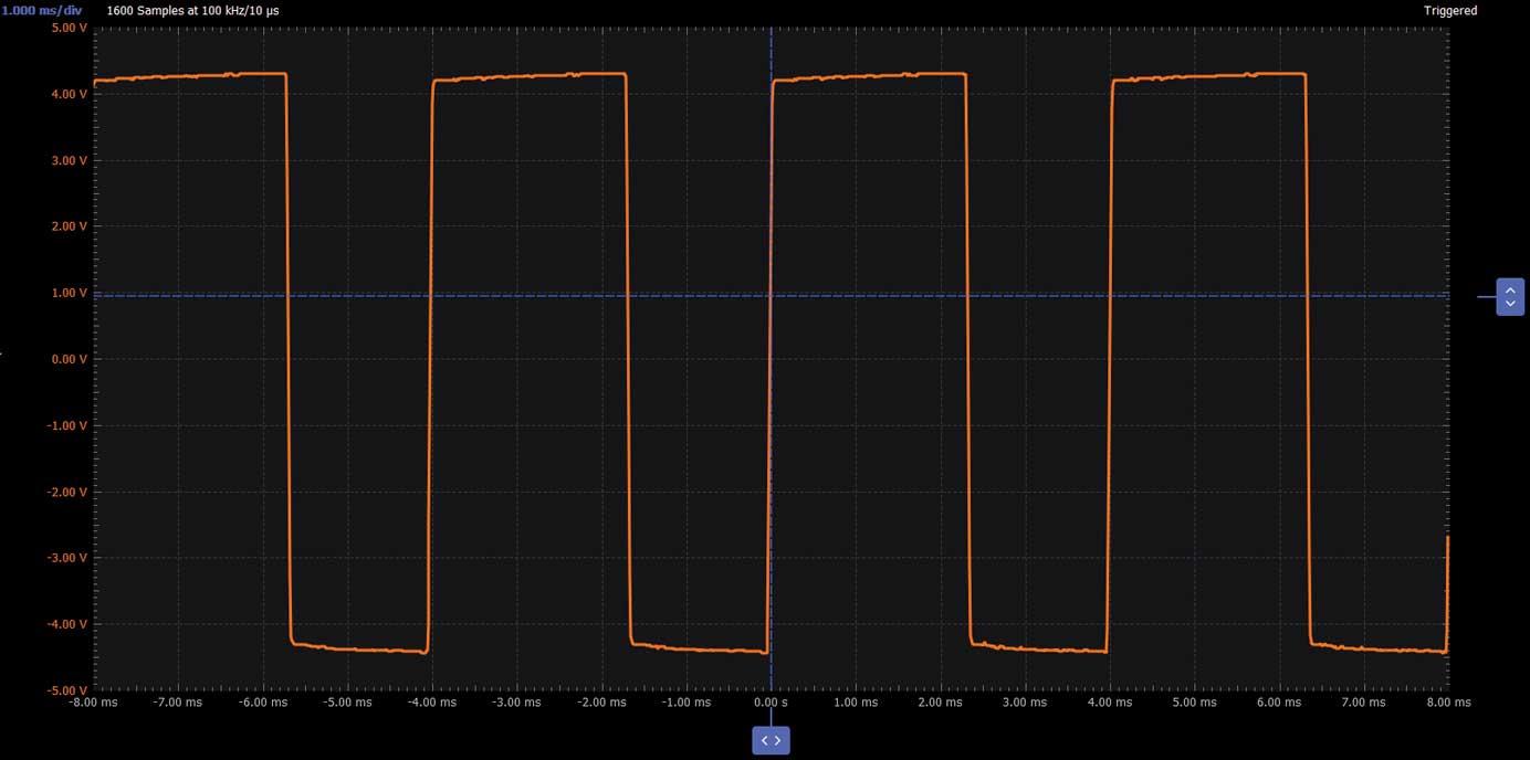
A plot of the output signal on Channel 2 of the scope is presented in Figure 6.
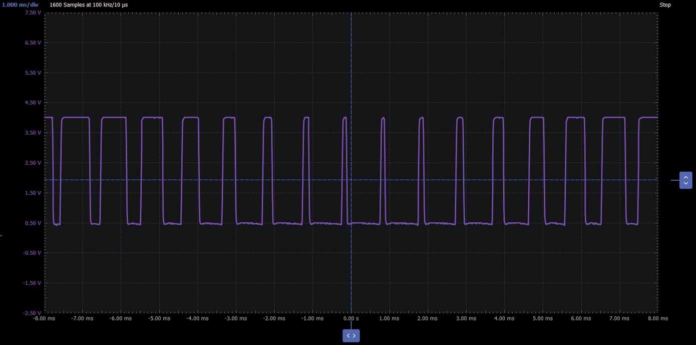
If the instantaneous magnitude of the modulation signal is greater than the carrier signal at a point in time, the output will be high. If the modulation signal is lower than the carrier signal, the output will be low.
If the peak of the modulation is less than the peak of the carrier signal, the output will be a faithful PWM representation of the modulation signal.
Pulse Width Control Using a DC Modulation Voltage
Background
For this particular application, we will use a simple operational amplifier in a switching mode configuration (see Activity: Op Amp as Comparator for further details) to demonstrate the pulse width modulation of a DC voltage.
Consider the circuit in Figure 7.
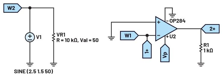
The circuit works as a simple comparator where the negative input of the operational amplifier is connected to the carrier waveform, while the positive input acts as a threshold voltage, which establishes when the transitions between high voltage output and low voltage output occur. The potentiometer acts as a voltage divider for the input reference voltage, adjusting the threshold voltage and implicitly the duty cycle of the output signal.
Hardware Setup
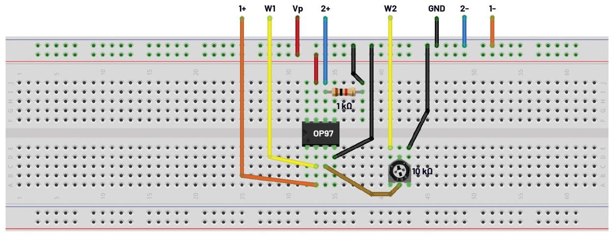
Build the breadboard circuit for pulse width control using a DC modulation voltage (Figure 8).
Procedure
Use the first waveform generator as source VIN to provide a 5 V amplitude peak-to-peak, 1 kHz triangle wave excitation to the circuit. Use the second waveform generator as a constant voltage source with 5 V amplitude peak-to-peak. Supply the op amp to +5 V from the power supply. Configure the scope so that the input signal is displayed on Channel 1 and the output signal is displayed on Channel 2.
An animated plot is presented in Figure 9.
The output signal is a PWM representation of the input voltage. Notice that, by varying the potentiometer value, the duty cycle of the signal changes, while the frequency remains constant.
Fixed 50% PWM with an Astable Multivibrator
Background
Consider the circuit in Figure 10.
The circuit shows an astable multivibrator using a single operational amplifier. The functionality is easy to understand while considering the functional principle of a Schmitt trigger (comparator circuit with hysteresis studied in Activity: Op Amp as Comparator): The input of the Schmitt trigger, which is identical to the inverting input of the operational amplifier, is connected to the output of the circuit via a resistor-capacitor network. While the capacitor voltage (which is also the input of the Schmitt trigger) is lower than the lower threshold, the output voltage equals the positive supply voltage of the circuit. Now the capacitor is charged via the resistor R3 until the upper threshold of the Schmitt trigger is reached. As a result, the output voltage of the operational amplifier is driven to the negative supply voltage. Now the capacitor is discharged via R3 until the voltage across the device reaches the lower threshold of the Schmitt trigger. The output voltage of the operational amplifier is driven to the positive supply voltage and the whole process starts again.
The advantage of this circuit is that it does not require an ADALM2000 to generate a carrier (but the duty cycle is fixed at 50%).
Hardware Setup
Build the breadboard circuit for PWM with an astable multivibrator (Figure 11).
Procedure
Supply the circuit to ±5 V from the power supply. Configure the scope so that the output signal is displayed on Channel 1.
A plot with the output signal on Channel1 of the scope is presented in Figure 12.
Note that the duty cycle of the output signal is approximately around 50% while the low/high voltage values tend to reach the positive/negative supply values.
Extra Activity
In the previous example, we generated a 50% fixed duty cycle PWM using astable multivibrators. But how can we adjust the duty cycle? For this, we will need to alter the circuit slightly.
Consider the circuit presented in Figure 13.
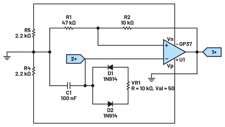
The resistor R3 in Figure 10 was replaced by a potentiometer and two diodes were inserted. Now the charging current of the capacitor is running through D1, while the discharging current is running through D2. Depending on the adjustment of the potentiometer VR1, the resistance of the charging current, running through the upper branch of the circuit, is different from that of the discharging current, running through the lower branch.
Hardware Setup
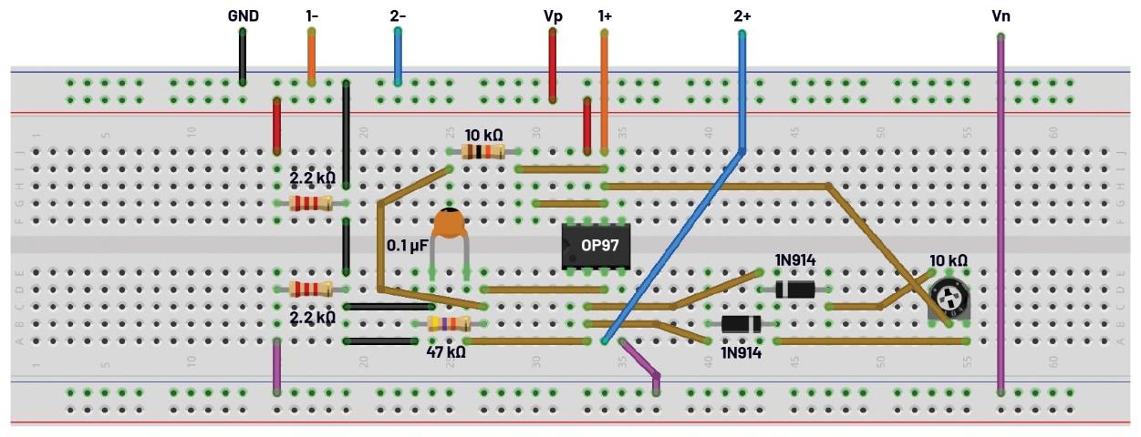
Build the breadboard circuit for adjusting the duty cycle for PWM with multivibrators (Figure 14).
Procedure
Supply the circuit to ±5 V from the power supply. Configure the scope so that the output signal is displayed on Channel 1 and the voltage on the capacitor (at the negative input of the op amp) is displayed on Channel 2.
Vary the potentiometer value and notice the duty cycle change. A plot example is presented in Figure 15.
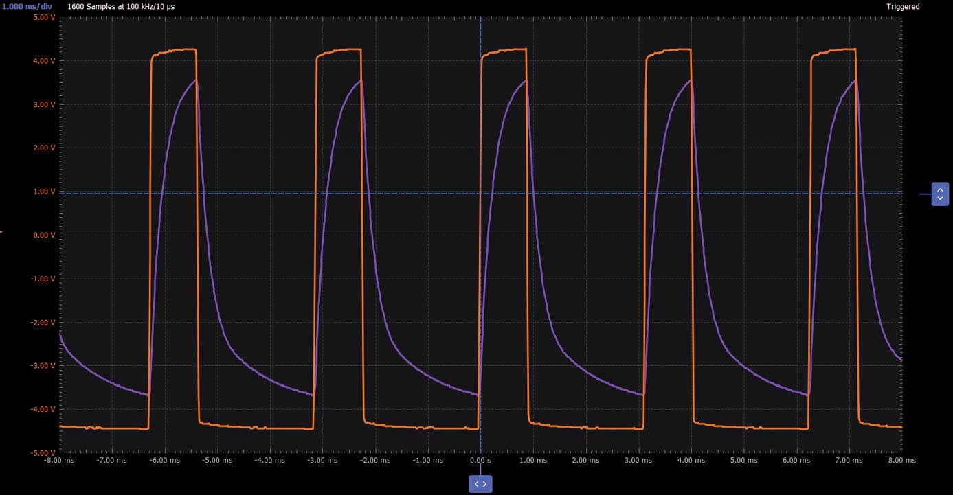
In this example, the duty cycle was set to around 25%. Whenever the duty cycle is altered, there is inevitably a slight variation in the switching frequency, because the two coupling networks at the inverting and noninverting input are both connected to the output of the operational amplifier.
Question
Can you list some practical real-world applications where pulse width modulation is effectively used?You can find the answer at the StudentZone blog.
About the Author
Antoniu Miclaus is a software engineer at Analog Devices, where he works on embedded software for Linux and no-OS drivers, as well as ADI academic programs, QA automation, and process management. He started working at ADI in February 2017 in Cluj-Napoca, Romania. He holds an M.Sc. degree in software engineering from the Babes-Bolyai University and a B.Eng. degree in electronics and telecommunications from the Technical University of Cluj-Napoca.


 combined with superior switching performance")


