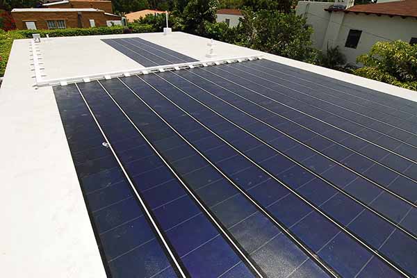
Thin film photovoltaics is an emerging class of alternatives to silicon photovoltaics. The use of thin film materials such as perovskite, organic, cadmium telluride (CdTe), and copper indium gallium selenide (CIGS) can broaden the application space for photovoltaics by offering advantages such as flexibility, lower costs, and reduced weight. It provides detailed analysis of the competing thin film PV technologies, along with determining their suitability for emerging applications such as indoor energy harvesting, powering Internet of Things devices and building integrated PV.
Emerging applications
The thin film photovoltaics market share has been steady at 5% of annual PV production for the past few years. However, the market is forecast to grow at a CAGR of 10% over the next 10 years to US$6.1 billion in 2033 following improvements to inefficiencies and manufacturing processes becoming cheaper and more streamlined. An additional stimulus is the development of new applications that conventional silicon PV is not suitable for due to its bulk, rigidity, and weight.
These applications include building integrated PV (BIPV), where the panels are attached to sides of buildings. In many cases, thin film PV panels can be up to 90 % lighter than silicon panels and therefore are particularly suitable for applications where weight is an important factor, such as on building façades or weak structures. Some types of thin film PV can be made semi-transparent, which makes them less aesthetically obtrusive and ideally suited to deployment on windows.
Other emerging applications belong to the small self-powered electronics and Internet of Things (IoT) sector, which is expected to grow substantially in the coming years as ‘smart’ electronics become ubiquitous in everyday life. Lightweight thin film minimodules can be used to power such devices and could serve as a cheaper and more long-lasting alternative to batteries or extensive wiring. Many household and retail appliances such as temperature, humidity, motion, and security sensors are likely to become increasingly ‘smart’ over the next decade and able to transmit data to the cloud to enable greater functionality. This is often referred to as the Internet of Things (IoT) and represents a substantial opportunity for thin film PV.
Technology overview and trends
- Overview of thin film photovoltaics and assessment of technological and commercial readiness levels.
- Individual assessment of perovskite, organic, dye sensitized, CdTe, CIGS, gallium arsenide, amorphous silicon, and copper zinc tin sulfide, and their suitability for widespread industry adoption.
- Evaluation of different manufacturing processes and barriers to entry.
- Benchmarking of solution-based deposition methods and substrate materials
- Trends in different thin film PV cell designs and compromises/factors to consider.
- Discussion of the biggest challenges facing each technology and where the greatest competition lies.
- Cost-effective alternatives to the different manufacturing process are discussed for each technology.
- Key innovation opportunities within the supply chain for emerging PV technologies are identified.
Market landscape
- Detailed overview of both established and emerging players in each thin film category including products, target markets, partnerships, and more.
- Analysis of the various addressable markets and their barriers to entry, technology gaps, drivers, and key users.
- Technology readiness, market status, and roadmap for key applications
- Detailed price comparisons and progressions of thin film PV
- Primary information from key companies based on one-to-one interviews, including multiple company profiles.
- 10-year market forecasts covering solar farm, building integrated PV, and wireless electronics applications, expressed in terms of production capacity and revenue.


