High-frequency switch mode circuits, such as those for power factor correction (PFC) using continuous conduction mode (CCM), require diodes that have low switching losses. For conventional silicon (Si) diodes in CCM mode, these switching losses result from the diode’s reverse recovery current due to stored charge in the diode junction during turn-off. Minimizing these losses generally requires an Si diode with a greater average forward current, leading to a larger physical size and higher cost.
A silicon carbide (SiC) diode is a better choice in a CCM PFC circuit because its reverse recovery current is only capacitive in nature. Reduced minority carrier injection in a SiC device means that the switching loss of a SiC diode is near zero. In addition, merged PIN Schottky (MPS) SiC diodes lower the device’s forward voltage drop, similar to a conventional SiC Schottky diode. This further minimizes conduction losses.
This article briefly discusses the challenge of low-loss switching in CCM PFC circuits. It then introduces an example MPS device from Vishay General Semiconductor – Diodes Division and shows how it can be applied to minimize losses.
Low-loss switching requirements
AC/DC switch mode power supplies with power ratings of over 300 watts typically use PFC to help meet international standards such as IEC61000-4-3, which specify reactive power and line harmonic levels. The diodes used in a PFC power supply, especially in switching power supplies operating at high frequency, must be able to handle the supply’s rated power and the related losses associated with the conduction and switching actions of the circuit. Si devices have noticeable reverse recovery losses. When an Si diode switches from a conducting to a non-conducting state, it remains conducting while charged carriers are removed from the junction. This results in significant current flow for the duration of the diode’s reverse recovery time, which becomes the Si diode’s turn-off loss.
The reverse recovery of SiC Schottky diodes is limited to capacitive discharge, which occurs more rapidly, effectively eliminating turn-off loss. SiC diodes have a higher forward voltage drop, which can contribute to conduction losses, but the drop can be controlled. SiC diodes also have the advantage of being able to handle a higher temperature range and faster switching. The higher temperature range allows greater power density, enabling smaller packages. The faster switching is due to the Schottky structure and the SiC’s shorter reverse recovery time. Operating at higher switching frequencies results in smaller inductor and capacitor values to improve volumetric efficiency in the supply.
The SiC MPS diode
The SiC MPS diode combines the useful features of both Schottky and PIN diodes. The structure results in a diode with fast switching, a low on-state voltage drop, low off-state leakage, and good high-temperature characteristics.
A diode using a pure Schottky junction offers the lowest possible forward voltage but is subject to problems at high currents, such as the surge currents in some PFC applications. MPS diodes improve the surge current performance by implanting P-doped areas beneath the metal drift zone of the Schottky structure (Figure 1). This forms a P-ohmic contact with the metal at the Schottky diode anode and a P-N junction with the lightly doped SiC drift or epi-layer.

Under normal conditions, the Schottky structure of the MPS diode conducts almost the entire current, and the diode behaves like a Schottky diode, with the attendant switching characteristics.
In the event of a high transient surge current, the voltage across the MPS diode increases beyond the threshold voltage of the built-in P-N diode, which begins to conduct, lowering the local resistance. This diverts current through the P-N junction regions, limiting the power dissipation and reducing the thermal stress in the MPS diode. This increase in conductivity of the drift zone at a high current keeps the forward voltage at a low value.
The surge current performance of SiC devices comes from the unipolar nature of the device and its relatively high drift layer resistance. The MPS structure also improves this performance parameter, and the P-doped area’s geometric placement, size, and doping concentration affect the final characteristics. The forward voltage drop is a compromise between the leakage and surge current ratings.
Under reverse bias, the P-doped regions force the overall area of maximum field strength downwards and away from the metal barrier with its imperfections and into the almost defect-free drift layer, thereby reducing the overall leakage current. This allows an MPS device to operate at a higher breakdown voltage with the same leakage current and drift layer thickness.
Vishay’s MPS structure uses thin-film technology where laser annealing is used to thin the backside of the diode structure, which reduces the forward voltage drop by 0.3 volts compared to earlier solutions. In addition, the forward voltage drops of the diodes are nearly temperature-independent (Figure 2).
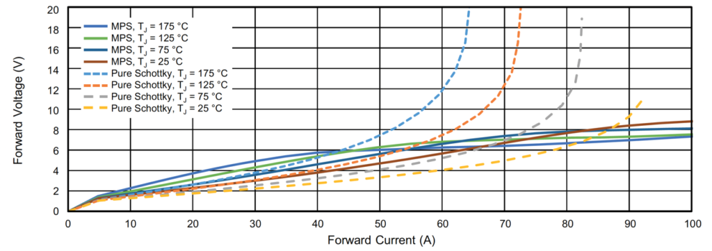
This plot shows the forward voltage of both types of diodes as a function of the forward current with temperature as a parameter. The forward voltage drops for the pure Schottky diodes increase exponentially for currents above 45 amperes (A). The MPS diode maintains a more consistent forward voltage drop with increasing forward current. Note that the forward voltage decreases with increasing temperature for higher forward current levels in the MPS diode.
Examples of MPS diodes
Vishay’s advanced SiC MPS diodes are rated for 1200 reverse peak volts with forward current ratings of 5 to 40 A. For example, the VS-3C05ET12T-M3 (Figure 3) is a through-hole-mounted diode in a TO-220-2 case and is rated for a forward current of 5 A, with a forward voltage of 1.5 volts at its full rated current. The diode’s reverse leakage current is 30 microamperes (mA), and it is rated for a maximum operating junction temperature of +175°C.
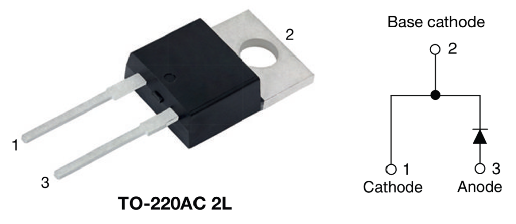
This diode family is the best choice for high-speed, hard-switching applications and delivers efficient operation over a wide temperature range.
MPS SiC diode applications
MPS diodes are typically applied in a wide variety of switched-mode power circuits, such as DC/DC converters, including those using full bridge phase shift (FBPS) and inductor-inductor-capacitor (LLC) topologies commonly found in photovoltaic applications. Another common application is in AC/DC power supplies utilizing PFC circuits.
The power factor is the ratio of active to apparent power and measures how efficiently incoming power is used in electrical equipment. A power factor of one is ideal. A lower power factor means that the apparent power is larger than the active power, which causes an increase in the current required to drive a specific load. High peak currents in loads with low power factors can also cause harmonics on the power line. Power suppliers generally specify the allowable range of the user’s power factor. AC/DC power supplies can be designed with PFC included (Figure 4).
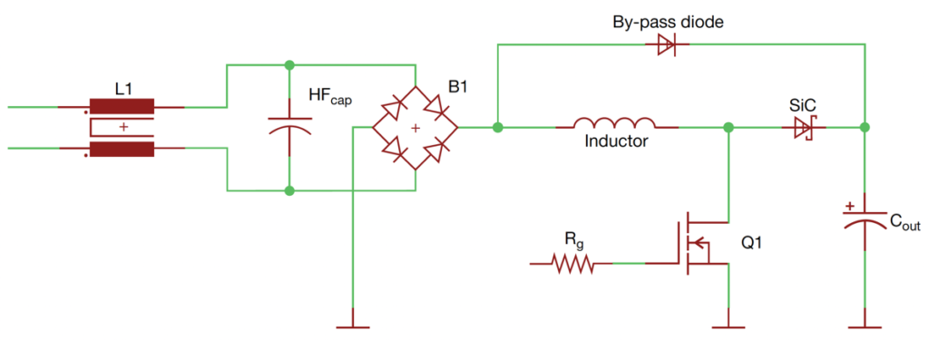
In Figure 4, the bridge rectifier B1 converts the AC input to DC. MOSFET Q1 is an electronic switch that is turned “on” and “off” by a PFC IC (not shown). While the MOSFET is “on,” the current through the inductor increases linearly. At this point, the SiC diode is reverse-biased by the voltage on the output capacitor (COUT),and the low reverse leakage of the SiC diode minimizes leakage loss. When the MOSFET is “off,” the inductor delivers a linearly decreasing current to COUT through the forward-biased output rectifier diode.
In a CCM PFC circuit, the inductor current does not fall to zero during the entire switching cycle. CCM PFCs are common in power supplies that supply several hundred or more watts. The MOSFET switch is pulse width modulated (PWM) by the PFC IC so that the input impedance of the power supply circuit appears purely resistive (a power factor of one), and the ratio of peak to average current, the crest factor, is kept low (Figure 5).
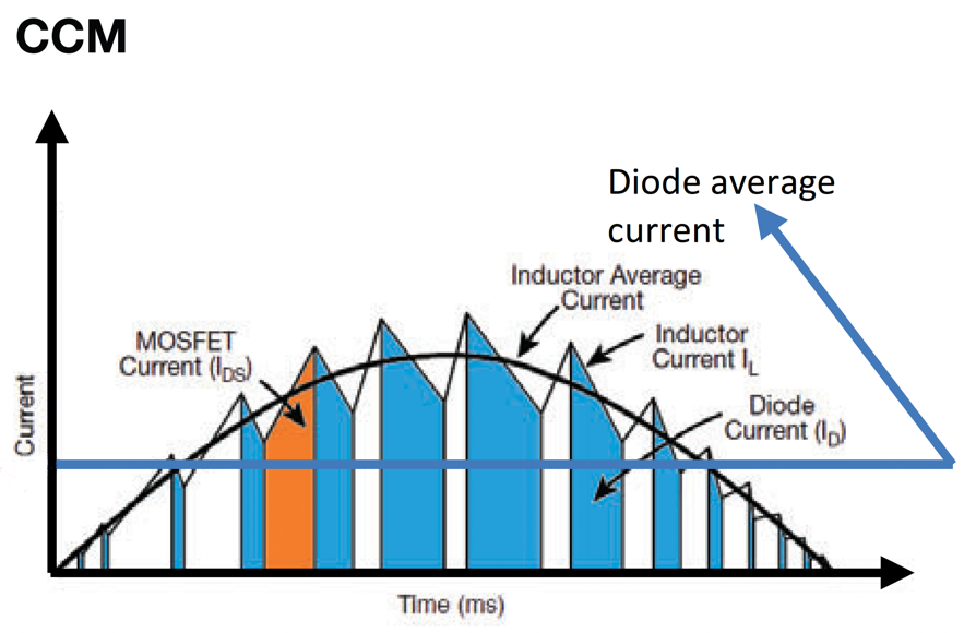
Unlike the discontinuous and critical current modes of operation where the inductor current reaches zero and the diode switches in an unbiased state, the inductor current in a CCM circuit never falls to zero so that when the switch changes state, there is a non-zero inductor current. When the diode switches into a reverse state, the reverse recovery contributes significantly to losses. Using an MPS SiC diode eliminates those losses. The decrease in switching loss due to using the MPS SiC diode brings the benefit of reducing chip size and cost for both the diode and the active switch.
Conclusion
Compared to Si, Vishay’s MPS SiC Schottky diodes offer higher forward current ratings, lower forward voltage drops, and reduced reverse recovery losses, all in a smaller package with higher temperature ratings. As such, they are well-suited for use in switched-mode power supply designs.


