


Introduction
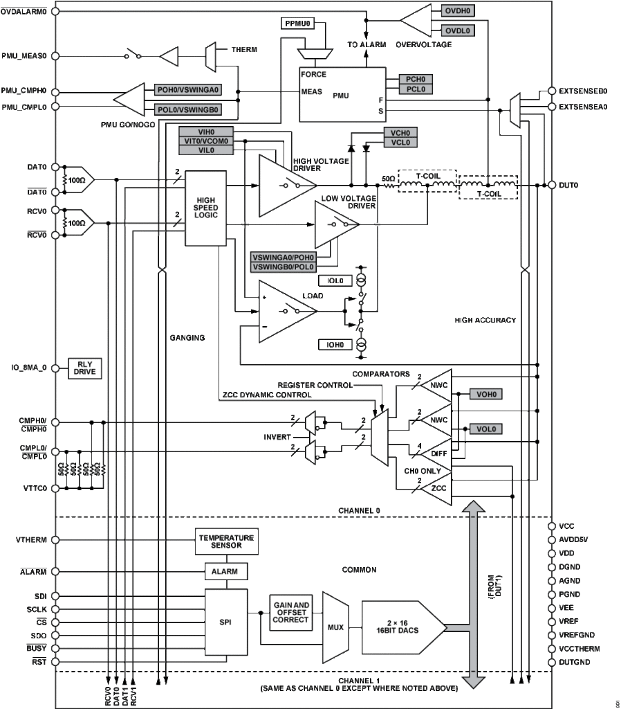
The ADATE334 is a complete dual-channel automatic test equipment (ATE) solution that performs the pin electronics functions of driver, comparator, and active load (DCL), and four-quadrant per pin parametric measurement unit (PPMU). Dedicated 16-bit DACs with on-chip calibration registers provide all necessary DC levels for operation of the device.
The high voltage driver features three active states: high (VIH), low (VIL), and terminate mode (VIT), as well as a high impedance inhibit state (HiZ). The inhibit state, in conjunction with the integrated dynamic clamps, facilitates significant attenuation of transmission line reflections when the driver is not actively terminating the line.
The open circuit drive capability is −1.5V to +7.0V to accommodate a wide range of ATE and instrumentation applications. The low voltage driver, working in conjunction with the high voltage driver, can provide 25mVpp to 600mVpp signals at up to 4.6Gbps in a 50Ω environment. Refer to the ADATE334 data sheet and functional block diagram for more information.
The MIPI Alliance provides a set of specialized physical layers with both complementary and unique features. MIPI C-PHY and MIPI D-PHY are mainly used for camera, display, and mobile applications. The ADATE334 high voltage and low voltage drivers can be used in combination to generate multilevel waveforms that are MIPI C-PHY and D-PHY compatible.
ADATE334 HIGH-SPEED MUX AND DRIVER CONTROLS
The ADATE334 utilizes internal high-speed multiplexers to map the high-speed inputs (DAT0, RCV0, DAT1, and RCV1) to the internal high voltage or low voltage driver control signals. The block diagram in Figure 1 shows the arrangement of the internal multiplexers and output drivers. The internal multiplexers (HV_DAT_x, HV_RCV_x, LV_VSWA_x, and LV_VSWB_x) generate the internal high-speed high voltage driver control signals (SELECTED_DAT_x and SELECTED_RCV_x) and low voltage driver control signals (SELECTED_VSWA_x and SELECTED_VSWB_x). Table 1 shows how the high voltage driver control signals determine the state of the high voltage driver output and Table 2 shows how the low voltage driver control signals determine the state of the low voltage driver output. The ADATE334 output is the sum of the high voltage driver and low voltage driver outputs.


 combined with superior switching performance")


