


The Semiconductor Inspection Systems Market is moving from being primarily a defect-detection business toward becoming a critical intelligence layer for modern semiconductor manufacturing. As chip geometries shrink, transistor structures become three-dimensional and advanced packaging becomes more complex, semiconductor manufacturers increasingly depend on inspection systems to identify defects, understand process variation and protect wafer yield.
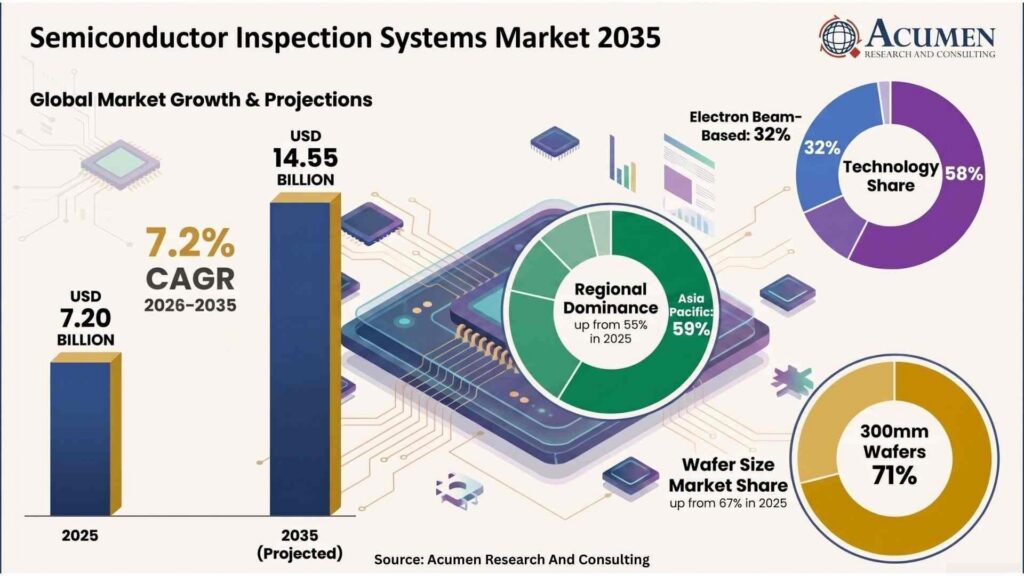
According to Acumen Research and Consulting, the Global Semiconductor Inspection Systems Market was valued at USD 7.20 billion in 2025 and is projected to reach USD 14.55 billion by 2035, representing a 7.2% CAGR from 2026 to 2035. Acumen’s latest analysis also shows that Asia Pacific accounted for 55% of the global market in 2025, while wafer inspection systems represented 54% and optical-based inspection held 58%.

Why Is the Semiconductor Inspection Systems Market Growing?
The fundamental growth driver is straightforward: semiconductors are becoming harder to manufacture without defects.
Advanced logic, DRAM, 3D NAND, high-bandwidth memory (HBM), AI processors and advanced packaging introduce increasingly demanding manufacturing conditions. Smaller process geometries leave less tolerance for particles, pattern abnormalities, scratches, contamination and process-induced defects.
Inspection systems therefore sit at a critical point in the semiconductor manufacturing workflow. They provide manufacturers with the data needed to determine whether a process is operating within specification and whether a detected anomaly could affect yield, reliability or device performance.
Acumen identifies increasing defect complexity at advanced semiconductor nodes as a major market driver. As inspection tools generate increasingly large volumes of defect candidates, manufacturers need faster ways to distinguish economically meaningful defects from nuisance signals.
This is where AI-powered semiconductor inspection is becoming particularly important.
AI Is Changing Semiconductor Inspection
Artificial intelligence is reshaping the Semiconductor Inspection Systems Market by shifting inspection from simple image acquisition toward automated interpretation.
Traditional inspection workflows can produce enormous numbers of potential defect candidates. Advanced-node optical inspection can generate substantially more candidates requiring review, creating a bottleneck if engineers must manually investigate every signal.
Machine learning and deep learning can help classify defect types, filter nuisance defects, prioritize candidates and correlate inspection results with manufacturing conditions. Acumen notes that AI is increasingly being used to distinguish real defects from spurious signals and to analyze high-dimensional inspection images.
The strategic opportunity is larger than automated classification. AI can potentially connect wafer inspection, metrology, equipment sensors and process-control data into a closed-loop manufacturing environment.
Instead of identifying a defect only after a process has produced it, AI-enabled systems can help manufacturers recognize patterns associated with process drift and support faster corrective action. This creates a path toward more autonomous semiconductor fabs.
Which Inspection Technologies Are Leading?
The Semiconductor Inspection Systems Market is increasingly divided between high-throughput optical inspection and high-resolution electron-beam approaches, with other technologies serving specialized requirements.
Optical-based inspection accounted for 58% of the market in 2025, according to Acumen, making it the leading technology segment. Its combination of speed and broad wafer coverage makes optical inspection particularly valuable in high-volume manufacturing.
Electron beam-based inspection accounted for 32%, supported by its higher resolution and growing importance in advanced-node manufacturing. Complex gate-all-around (GAA) transistor structures, advanced DRAM, 3D NAND and other sophisticated architectures require increasingly detailed defect analysis.
The industry is therefore unlikely to converge on a single inspection technology. Instead, fabs will increasingly use complementary optical, e-beam, X-ray, ion-beam and hybrid or multimodal approaches depending on the manufacturing stage and defect characteristics.
Wafer Inspection Remains the Largest Application
Wafer inspection systems held a 54% share of the Semiconductor Inspection Systems Market in 2025, according to Acumen, making wafer inspection the largest system-type segment. Acumen expects the segment to maintain a leading 53% share by 2035.
The reason is structural. Inspection is required throughout semiconductor wafer production, including lithography, deposition, etching, implantation, cleaning and pattern formation.
At advanced nodes, even a small process variation can affect yield across large numbers of dies. Consequently, manufacturers are increasing their reliance on high-speed, high-resolution wafer inspection equipment, defect inspection systems and automated defect classification.
Mask and reticle inspection is another important area. Acumen estimates that mask and reticle inspection systems accounted for 20% of the market in 2025, reflecting the importance of photomask quality as advanced and EUV-based lithography becomes more sophisticated.
Why Are 300 mm Wafers Important?
The transition toward higher-volume 300 mm manufacturing continues to shape demand for semiconductor inspection equipment.
According to Acumen, 300 mm wafers represented 67% of the market in 2025, and their share is projected to rise to 71% by 2035. The growth is linked to investment in advanced logic, memory, AI processors, high-performance computing and high-volume semiconductor manufacturing.
At the same time, 200 mm wafers remain strategically important for mature-node applications. Acumen estimates that 200 mm wafers represented 23% of the market in 2025, supported by automotive semiconductors, power devices, analog chips, MEMS, sensors and industrial electronics.
This means inspection suppliers must serve two different manufacturing realities: extreme precision at leading-edge nodes and cost-efficient quality control across mature-node production.
Which Companies Are Leading the Semiconductor Inspection Systems Market?
The competitive landscape is concentrated around a small number of highly specialized semiconductor equipment companies.
KLA Corporation is one of the most important global suppliers, with capabilities spanning optical inspection, electron-beam inspection, defect review, metrology and process-control analytics.
Applied Materials combines inspection and metrology with a broader semiconductor equipment portfolio. Its systems increasingly incorporate data analytics and AI-based approaches for defect classification and process optimization. Applied Materials is headquartered in Santa Clara, California, and operates globally across major semiconductor manufacturing regions.
ASML is particularly important to advanced lithography and semiconductor process control, with inspection and metrology technologies closely connected to the requirements of leading-edge patterning.
Hitachi High-Tech has a strong position in electron-beam-based semiconductor inspection, measurement and analysis, particularly where high resolution is required.
Other significant companies include Onto Innovation, Lasertec, Camtek, SCREEN Semiconductor Solutions, Advantest, Nova and ZEISS. Current industry research identifies these companies among the major participants across optical inspection, e-beam inspection, metrology, mask inspection and advanced packaging inspection.
Onto Innovation is particularly notable for combining wafer inspection, metrology, defect inspection, analytics and advanced packaging technologies. The company is headquartered in Wilmington, Massachusetts, and maintains a worldwide sales and service organization.
Camtek focuses on high-end inspection and metrology covering front-end and mid-end processes through post-dicing inspection, with customer support infrastructure spanning the U.S., Europe and major Asian semiconductor markets.
Which Regions Have the Highest Concentration of Inspection-System Companies?
There is an important distinction between where inspection-system companies are headquartered and where semiconductor inspection demand is concentrated.
Asia Pacific is the dominant demand center. Acumen estimates that the region held 55% of the Semiconductor Inspection Systems Market in 2025, with its share projected to rise to 59% by 2035. The regional market is expected to expand from approximately USD 4.27 billion in 2026 to USD 8.58 billion by 2035, representing an 8.1% CAGR.
Taiwan: Advanced Foundry Concentration
Taiwan is arguably the most strategically important location for advanced semiconductor inspection demand because of its concentration of leading-edge foundry manufacturing.
The country’s semiconductor equipment investment supports demand for optical inspection, e-beam inspection, critical-dimension metrology, overlay measurement and mask/reticle inspection.
South Korea: Memory and Advanced Logic
South Korea is another major inspection-equipment hub, driven by Samsung and SK hynix. Acumen notes approximately USD 21.5 billion in semiconductor equipment spending was projected for South Korea in 2025, supporting demand for wafer inspection, e-beam systems and metrology across DRAM, NAND and advanced logic manufacturing.
Japan: Equipment Technology and Semiconductor Manufacturing
Japan has a unique position because it combines semiconductor manufacturing with a deep domestic semiconductor equipment ecosystem. Lasertec, headquartered in Yokohama, is a prominent Japanese developer and manufacturer of semiconductor-related inspection systems.
Other important Japanese participants include Hitachi High-Tech, Tokyo Electron and Advantest.
China: Scale and Domestic Equipment Development
China’s enormous semiconductor manufacturing-equipment investment base makes it a major source of inspection demand. Acumen cites approximately USD 38 billion in semiconductor manufacturing equipment investment projected for China in 2025. Capacity expansion across mature-node logic, power semiconductors, memory and other applications is supporting demand for inspection technologies.
Export controls affecting advanced semiconductor equipment are also encouraging greater development of domestic semiconductor manufacturing technologies, including inspection capabilities.
United States: Technology Leadership and Fab Expansion
North America accounted for 29% of the Semiconductor Inspection Systems Market in 2025, according to Acumen. The regional market is forecast to increase from approximately USD 2.25 billion in 2026 to USD 3.93 billion by 2035, representing a 6.4% CAGR.
The United States has a particularly strong concentration of semiconductor equipment and process-control companies, including KLA, Applied Materials and Onto Innovation. The expansion of domestic fabs adds another source of demand for inspection and process-control equipment.
India Is Becoming an Emerging Inspection Market
India is not yet comparable with Taiwan, South Korea, Japan or China in semiconductor inspection-system demand, but its strategic importance is increasing.
Acumen reports that India has more than 12 approved semiconductor manufacturing units with cumulative investment exceeding ₹1.64 lakh crore. As fabs and OSAT/ATMP facilities develop, demand is expected to emerge for wafer inspection, metrology, package inspection and testing equipment.
This makes India a market to watch rather than a current global concentration center.
The Next Competitive Battleground: AI-Enabled Closed-Loop Inspection
The next phase of the Semiconductor Inspection Systems Market will be determined not simply by who can detect the smallest defect, but by who can convert inspection data into actionable manufacturing intelligence.
AI can help connect defect images with equipment parameters, process recipes, historical yield information and metrology results. That creates opportunities for predictive defect detection, automated defect classification, predictive maintenance, process drift detection and closed-loop process control.
However, deploying AI in a high-volume fab presents challenges. Models must remain reliable as materials, recipes, device structures and process conditions change. Acumen highlights the difficulty of transferring strong AI performance from controlled environments into high-volume manufacturing, particularly where false positives increase review workloads and missed defects can directly affect yield.
What Is the Outlook for the Semiconductor Inspection Systems Market?
The long-term outlook remains constructive. Acumen projects the global Semiconductor Inspection Systems Market to grow from USD 7.20 billion in 2025 to USD 14.55 billion by 2035 at a 7.2% CAGR.
Growth will be supported by advanced-node manufacturing, AI processors, HBM, 3D NAND, advanced packaging, expanding foundry capacity and continued investment in semiconductor fabs.
The industry’s center of gravity will remain strongly anchored in Asia Pacific, while the United States and Europe retain important technology and equipment-development roles. Japan and South Korea will remain critical to inspection and semiconductor equipment innovation, while China and India are likely to influence the industry’s next phase through capacity expansion and localization.
Ultimately, semiconductor inspection systems are becoming more than quality-control tools. They are evolving into data-driven process-intelligence platforms. As semiconductor manufacturers pursue smaller geometries, higher yields and increasingly complex architectures, the companies capable of combining inspection physics, automation, analytics and artificial intelligence will be best positioned to shape the next generation of semiconductor manufacturing.