


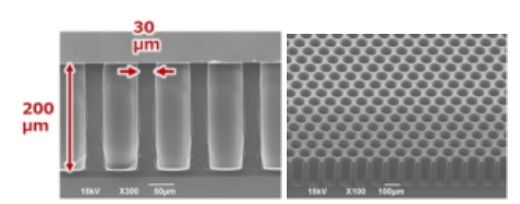
Toray Industries, announced that it has developed the STF-2000, a photosensitive polyimide solution that enables high-aspect-ratio fine patterning with 30-micrometer line widths in films up to 200 micrometers thick. This breakthrough came from applying advanced high-sensitivity negative-tone formulation and proprietary photoresist design technology, which controls curing stress (see Figure 1).
This new material retains the inherent advantages of a polyimide structure. These include excellent resistance to heat and chemicals, mechanical strength, insulation, and X-ray durability. At the same time, it enables fine microfabrication with aspect ratios of up to 7. Sustainability also informed the STF-2000’s engineering. It is free of N-Methyl-2-pyrrolidone (NMP; see glossary note 1) and per- and polyfluoroalkyl substances (PFAS; glossary note 2), helping shrink the environmental footprints of electronic components, micro electromechanical systems (MEMS; glossary note 3) devices, and other applications while supporting their high performance. While the standard formulation of this material is as a solution, Toray is developing a thick-film sheet version. Customer evaluations are underway with a view to commercialization during fiscal 2025. Toray will continue striving to cater to diverse needs.
Ongoing efforts in recent years to develop high-performance electronic products have fueled demand for microfabrication techniques to miniaturize and more densely integrate electronic components and for structural materials that support diverse designs. Demand is particularly strong for photosensitive materials that allow fine processing, even with thick films, while preserving the performance advantages inherent to polyimide structures.
While engineers have long relied on photolithography (glossary note 4) to microfabricate electronic components and MEMS devices, using it with thick-film photosensitive materials has presented four key challenges that STF-2000 overcomes.
1. Deformation and cracking: Once thickness exceeds 100 micrometers, shrinkage stress during curing becomes significant, often causing deformation or cracks in cured materials.
2. Incomplete ultraviolet curing: Photosensitive components tend to absorb ultraviolet light at the film surfaces. As films become thicker, light penetration decreases, making it harder to cure material properly and reducing patterning performance.
3. Inadequate development: High aspect ratios require more time to fully remove undeveloped areas in fine features. This can leave residual film in via patterns and cause warping, wrinkling, or other distortion in pillar, stripe, and grid structures.
4. Foreign particles and interlayer delamination: Thick-film photolithography conventionally stacks and exposes multiple thin-film sheets. Stacking increases the risk of foreign particle contamination and delamination between layers, however, threatening production efficiency.
While offering excellent resistance to water, oil and heat, PFAS have become a growing concern in recent years because of their persistence in the environment and potential risks to human health. Pressure has accordingly increased to develop sustainable materials that address environmental and social issues. Toray formulated STF-2000 without PFAS and adopted an alkaline development process that avoids organic solvents. It thus helps reduce environmental impact and support the transition to a more sustainable economy.
Applying the new material to form thick films could enhance insulation of electronic components and support high-aspect-ratio wiring. In structural material applications, it will offer engineers greater design flexibility for microstructures using photolithography so they
-2 / 5-
can develop more advanced MEMS devices. The material will simplify manufacturing by forming thick-film patterns through a single coating, exposure, and development step, thus boosting productivity and helping cut process costs.
This material also delivers high-resolution patterning with line/space ratios of 4 micrometers or less in the 10–30 micrometer film thickness range traditionally served by conventional polyimides.
Toray will fully leverage its core capabilities in synthetic organic chemistry, polymer chemistry, biotechnology, and nanotechnology in pursuing R&D into groundbreaking materials that can drive fundamental change in keeping with its enduring commitment to delivering new value and contributing to social progress.
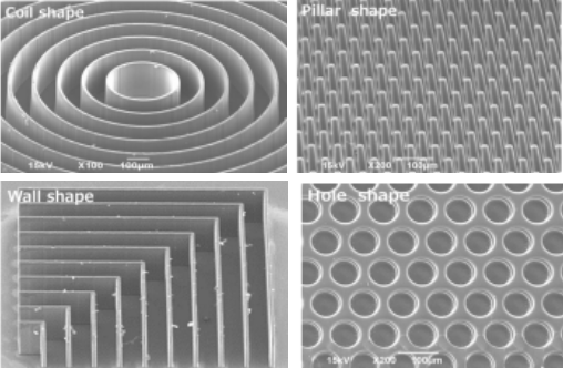
Figure 2. Examples of thick film and high aspect ratio processing
This photosensitive polyimide material can form various patterns using a standard exposure system with an h-line process
-3 / 5-
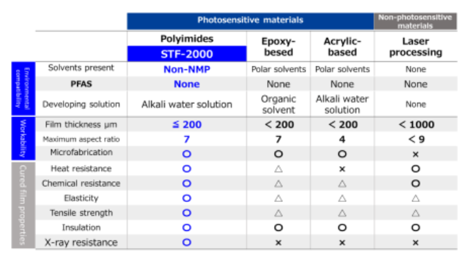
Performance comparisons of STF-2000 and other materials
Glossary
1. The chemical, electronics, pharmaceutical, and other industries rely heavily on NMP for its high solubility. It plays a role in manufacturing high-performance resins such as polyamides and polyurethanes, as well as in paints, adhesives, and lithium-ion battery electrode materials. Its drawback is that the body can absorb it, potentially affecting the central nervous system, bone marrow, liver, testes, kidneys, and adrenal glands. It is thus a restricted substance under Entry 71 of Annex XVII of the Registration, Evaluation, Authorisation and Restriction of Chemicals, a European Union regulation, and requires careful handling.
2. PFAS offer excellent heat resistance and stability, and are used in diverse range of products. Some of these compounds have raised concerns because of their environmental and human health risks. They are thus subject to water quality regulations and manufacturing restrictions.
3. MEMS technology integrates micro-mechanical components, sensors, actuators, and other elements using microfabrication techniques developed for semiconductor devices.
4. Photolithography entails coating substrates with photosensitive materials, exposing them to light to form circuit patterns. This technique is ubiquitous in manufacturing semiconductors and liquid crystal displays.


 combined with superior switching performance")


