Kawasaki, Japan : Subtle, extremely low idle current [1] load switches produce huge improvements in IC performance
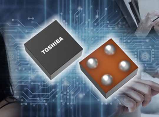
Toshiba Electronic Devices and Storage Corporation has introduced the “TCK12XBG Series” of load switch ICs to the market. It provides a significant reduction in idle current [1] and an output current rating of 1A. Encapsulated in a tiny WCSP4G package, these new ICs help product manufacturers to innovate a new generation of wearables and IoT devices that consume less power and provide longer charging times. Bulk shipments start today.
The TCK12XBG Series N uses a new driver circuit that produces a typical on-state idle current of 0.08nA [1] . This represents an area of 99.9% reduction from Toshiba’s current product, “TCK107AG”. This is a tremendous advance in efficiency that will help small battery-powered wearables and IoT devices last longer.
The WCSP4G, a new package developed for these products, is only 0.645×0.645mm, about 34% smaller than the TCK107AG. Due to its small size, it is easy to mount it on small boards. Its back layer can reduce damage to the microchip in the process of mounting it to the board.
Toshiba has designed a series of three ICs: the TCK127BG with automatic discharge that turns on at active high; Automatic non-discharge TCK126BG that turns on active high; and TCK 128BG with automatic discharge that turns on at active low.
Toshiba will continue to improve low passive current technology to reduce device size, reduce power consumption, and drive a sustainable future.
Experiment
- Wearables, IoT devices, smartphones (on and off switches for power supplies for sensors, etc.)
- Replacement of load switch circuits formed by discontinuous semiconductors, such as MOSFETs (MOSFETs), transistors, etc.
Properties
- Extremely low idle current (on state) [1] : I Q =0.08nA (typ)
- Low standby current (in OFF state): I Q(OFF) +I SD(OFF) =13nA (Typ)
- Small WCSP4G Package: 0.645×0.645mm (Typ), t:0.465mm (Max)
- back layer that minimizes damage during board plating
note:
[1] 1 mm 2 or between the load switch with a small package of reduced size Aisij and output current rating of 1A. Toshiba’s survey for January 2022.
| Key Specifications | |||||
| (Unless otherwise specified, @T a =25°C) | |||||
| part number | TCK126BG | TCK127BG | TCK128BG | ||
| package | Name | WCSP4G | |||
| Size Type (MM) | 0.645×0.645, t:0.465 (max) | ||||
| assured maximum ratings | Input voltage V IN (V) | 0.3 to 6.0 | |||
| Control Voltage V CT (V) | 0.3 to 6.0 | ||||
| Output Current I OUT (A) | DC | 1.0 | |||
| Pulse | 2.0 | ||||
| Power dissipation P D (W) | 1.0 | ||||
| operating range (@T a_opr = -40 to 85°C) | Input voltage V IN (V) | 1.0 to 5.5 | |||
| Output Current I OUT max (A) | 1.0 | ||||
| electrical characteristics | Idle Current (On State) I Q type . (nA) | @V IN =5.5V | 0.08 | ||
| Standby Current (Off State) I Q(OFF) + I SD(OFF) typ. (nA) | @V IN =5.5V | 13 | |||
| on resistance R ON type . (mΩ) | @V IN = 5.0V, I OUT = -0.5A | 46 | |||
| @V IN = 3.3V, I OUT = -0.5A | 58 | ||||
| @V IN = 1.8V, I OUT = -0.5A | 106 | ||||
| @V IN = 1.2V, I OUT = -0.2A | 210 | ||||
| @V IN =1.0V, I OUT = -0.05A | 343 | ||||
| AC Characteristics | V OUT rise time t r typ. (μs) | @V IN =3.3V | 363 | 363 | 363 |
| V OUT fall time t f typ. (μs) | 125 | 32 | 32 | ||
| Turn on delay t ON typ. (μs) | 324 | 324 | 324 | ||
| Turn off delay t OFF typ. (μs) | 10 | 10 | 10 | ||
| auto-discharge function | , | embedded | embedded | ||
| on/off control logic | active high | active high | active low | ||
| Sample checking and availability | buy online | buy online | buy online |
Find out more about the new product at the following links:
TCK126BG
TCK 127BG
TCK 128BG
For more information on Toshiba’s various load switch ICs, follow this link:
loadswitch IC
For information on availability of new products with online distributors, refer to the following links:
TCK126BG
TCK 127BG
TCK 128BG


