


Abstract
This article details the design considerations when upgrading an existing GMSL2 design to a GMSL3 design. The specific examples use a GMSL2 sensor pair, the MAX96717 and MAX96716A, and a pin-for-pin compatible GMSL3 sensor pair, the MAX96793 and MAX96792A. The article covers the benefits of GMSL3 along with design considerations for upgrading from GMSL2 to GMSL3.
Introduction
One of the primary benefits of the GMSL technology is the intergeneration compatibility between devices within one generation. GMSL2 is backwards compatible with GMSL1 and GMSL3 is backwards compatible with GMSL2; verify the part’s compatibility by using the data sheet. This flexibility also translates to time savings by maintaining the same pin and package to reuse designs for compatible parts.
GMSL3 Overview
The main difference with GMSL3 is doubling the GMSL data rate on the link up to 12Gbps. GMSL2 is typically sufficient for most applications, however, sensor and display bandwidths continue to increase. GMSL3 aims to achieve these higher data rates while maintaining all the benefits of GMSL, including adaptive equalization (AEQ), ASIL-B functional safety, and robust error monitoring diagnostics.
GMSL2 uses non-return to zero (NRZ) modulation which has a Nyquist frequency of half the transmission data rate. This translates to 3GHz for a 6Gbps link (or 1.5GHz for a 3Gbps link). Doubling the data rate while still using NRZ modulation translates to 6GHz for a 12Gbps link. However, there are disadvantages for using this higher frequency such as more insertion loss on the cable, connector, and PCB to reduce the total cable length of the application.
To avoid a higher frequency for double the data rate, GMSL3 leverages pulse-amplitude modulation 4 level (PAM4) to maintain the same Nyquist frequency as GMSL2. The lower operating frequency on the channel delivers many system benefits:
- GMSL2 and GMSL3 utilize the same clock link rate for schematic and layout reuse, operating on FR-4 PCBs.
- There is lower insertion loss on cables and connectors.
- Higher spectral efficiency by doubling the bandwidth and maintaining the same link rate.
The GMSL3 supports both 6Gbps with NRZ and 12Gbps with PAM4.
Design Considerations
To demonstrate, consider the MAX96793 CSI-2 to GMSL3 serializer and the MAX96792A GMSL3 to CSI-2 deserializer. In general, the changes are minimal but need to be reviewed for each system application.
Pin-for-Pin Compatibility
GMSL devices between GMSL2 and GMSL3 generations are designed to be pin-for-pin compatible for design reuse. The serializer packages are 5mm x 5mm TQFN devices. Figure 1 details the pinouts of the MAX96717 and MAX96793:
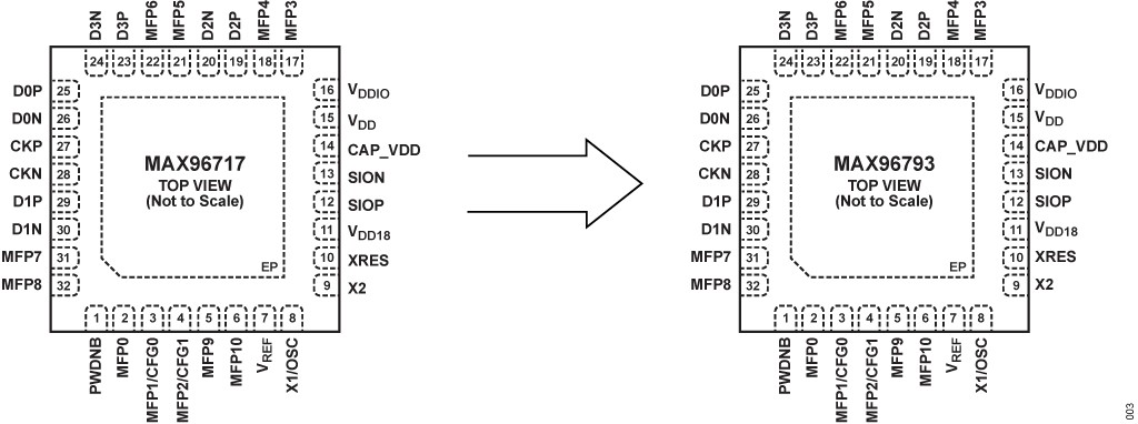
When using the reference clock over reverse (RoR) capability on these devices, connect a 20nF± 10% capacitor between the VREF pin (pin 7) and ground. This connection is required for GMSL3 mode when using RoR and optional for GMSL2 mode to maintain optimal reverse link margin.
If RoR is not being used on GMSL3, this capacitor is not required.
The deserializer packages are 7mm x 7mm TQFN devices. Figure 2 details the pinouts of the MAX96716A and MAX96792A:

Power Consumption
Power consumption of these devices is characterized by using the physical layer interfaces to their full, operational capacity as detailed in the Configuration column of Table 1.


 combined with superior switching performance")


