


Increasing power density and shrinking power supplies are nothing new. This trend is projected to continue, enabling new markets, applications, and products. This blog introduces design engineers to how STMicroelectronics (ST) power solutions incorporate wide bandgap (WBG) technology to help drive the device miniaturization trend.
The Importance of Higher Power Density
Higher power density is vital to meeting the increasing energy demand everywhere and the ongoing market needs for smaller and more efficient power supplies. Semiconductor suppliers have managed to get a lot of utilization out of standard silicon-based devices, and silicon-based devices will continue to be a significant part of power systems. However, wide bandgap semiconductor materials have substantial advantages for achieving the most compact and efficient power solutions. Gallium Nitride (GaN), for example, is a powerful solution to address these challenges and advance power density and miniaturization capabilities. ST has used GaN technology in its innovative MasterGaN family of devices. MasterGaN can be applied to a resonant LLC converter to create a heatsink-less 250W power supply.
GaN
As a wide bandgap semiconductor, GaN power FETs feature greater power density and can work at higher voltages, operate at higher frequencies, and enable smaller devices. The critical phenomenon that differentiates GaN from traditional silicon (Si) semiconductor devices is its higher bandgap. The bandgap is the energy needed to excite an electron to have it jump from the top of the valence band to the bottom of the conduction band, where it can be used in the circuit. Increasing the bandgap has a significant impact on that device.
Materials like GaN that have a larger bandgap can withstand stronger electric fields. This robustness allows GaN to operate at higher voltages and higher electron mobility and saturation velocity. These key attributes make GaN switches ten times faster and significantly smaller at the same resistance and breakdown voltage as equivalent silicon components. GaN power FETs are sparking power engineering with their increased speed, efficiency, and power density that are way beyond the capabilities of traditional silicon MOSFETs. Market demand for greater efficiency and power density is pushing the adoption of GaN in compact, portable, and high-power applications. Powerful chargers are a key growth area for fast charging smartphones, tablets, and mobile applications. GaN has many other applications that would greatly benefit from its capabilities, such as EV charging, telecom, and high-power server applications.
Solving Design Challenges with MasterGaN
Discrete GaN transistors traditionally require dedicated high voltage half-bridge gate drivers that take up a significant amount of board space. The discrete approach also introduces additional inductance and capacitance on the highly sensitive GaN gates. MasterGaN solves these design challenges through the package-level integration of gate drivers with GaN transistors. ST’s MasterGaN product family combines high-voltage smart-power BCD-process gate drivers with high-voltage GaN transistors in a single package. The MasterGaN family has three key attributes: Compactness, Robustness, and Ease of Design. MasterGaN achieves compactness due to its high-power density; it is ¼ the size of a comparable silicon solution. The MasterGaN devices are robust and include an offline driver optimized for GaN High Electron Mobility Transistors (HEMT). The straightforward design is an innovative solution in a 9mm x 9mm quad flat no-lead (QFN) package that can reduce system size by up to 70 percent, enabling chargers and adapters to be up to 80 percent lighter.
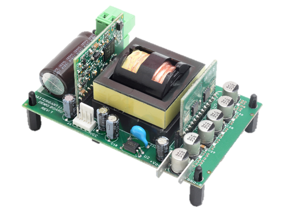
By leveraging the high level of integration of MasterGaN, it is possible to create a 250W compact, highly efficient switch mode power supply without heatsinks (Figure 1). The power supply offers an excellent example of reducing space on a power supply design. The board is architected as a mainboard with two vertical daughter cards. The daughter card on the left is the MASTERGAN1 circuit, while the one on the right is the synchronous rectifier circuit for the secondary side. The design includes short circuit, overload, brownout, and overvoltage protection. The ST L6599A resonant LLC controller in this design runs at a frequency of 160kHz, although the controller can run up to 700kHz, and the design features integrated gate drivers with a 15V output drive. MasterGaN is entirely compatible with the L6599A due to its wide input-voltage range and high-frequency capability. This design also includes an SRK2001 LLC resonant controller. When combined with standard silicon MOSFETs, this controller helps maximize power-supply efficiency by reducing output losses.
When designing with high-performance switched-mode power supplies, designers must exercise care to ensure all power supply pins are correctly fed and decoupled. Designers also need to make sure control signals are correctly configured to extract the full benefits of GaN.
Thermal management is also essential, and ST has some tips to optimize board layout to keep things running cool. MasterGAN features three sets of supply pins: a front-end supply (VCC), a floating high-side supply (BOOT), and a low-side (PVCC) supply. Note that both low- and high-side drivers are floating. Combined with the integrated level shifters, these floating supplies help ensure proper gate drive by making the input signals insensitive to the inductive noise coupling that would result if the two grounds were connected. These three supplies can all be powered independently, although, in many applications, the high-side driver can be supplied by VCC through the integrated Bootstrap Diode. This bootstrap structure is turned on during low-side ON time only. This structure reduces the component count in medium frequency (up to typically 400kHz) applications. As the switching speed increases, consider powering through an external higher performance bootstrap diode. Supply source basics are shown in (Figure 2).
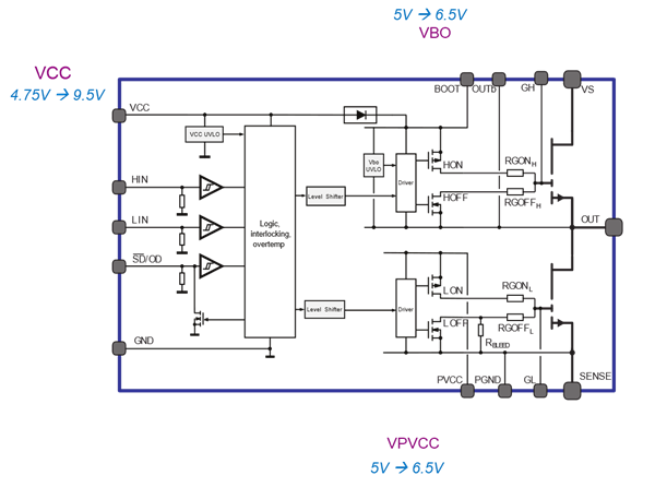
MasterGaN input logic was explicitly designed to make driving GaN transistors as straightforward as possible. For MasterGaN, the upper voltage limit of the input pins is 20V regardless of the VCC value. This feature makes it easy to use MasterGaN with a “MOS-oriented” controller that operates at a typical VCC of 12V or more, as in the L6599A in the design example. The thresholds also allow MasterGaN to be connected to a microcontroller with 3.3V logic for implementing your own custom SMPS algorithm. There’s not much more to it when connecting the control signals to MasterGaN than making sure they are connected! One could add a low-pass filter to the signal path to eliminate the risk of accidental switching if the system is noisy. MasterGaN devices internally buffer logic inputs (LIN, HIN, and SD/OD) with Schmitt triggers with an accurate turn-on/turn-off threshold to improve noise immunity and increase the repeatability of the propagation delays. Internal pulldown resistors in the MasterGaN devices avoid undefined voltage levels when logic inputs are high impedance.
Thermal Management in Power-Supply Design
Thermal management is among the most critical aspects of power-supply design and board layout. The 9mm x 9mm dual-flat no-leads (DFN) package features three exposed pads that must be soldered to the circuit board. Thermal resistance to the top case is much higher than to the exposed pads on the bottom. This design facilitates the removal of heat through the PCB and copper-pour areas (Figure 3).
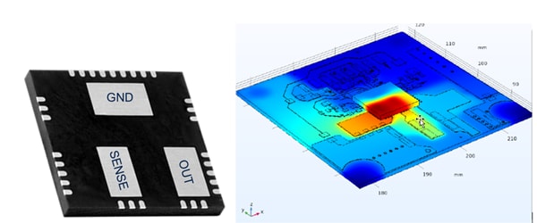
On the MasterGaN circuit, the current-carrying GAN transistors are beneath the large pads labeled SENSE and OUT. These are the heat-critical locations of the package. Pay close attention to maximizing heat extraction when laying out the board. OUT is connected to the high-side transistor source, while SENSE is connected to the low-side transistor source. In addition to the EVLMG1-250LLC LLC demo board here, ST has other evaluation platforms to help designers prototype, test, and develop high-performance power supplies. EVALMASTERGAN1 and 2 are available now, as well as the EVLMG1-250WLLC.
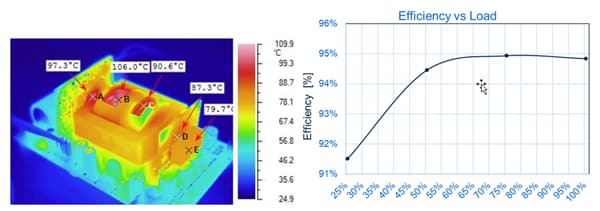
The EVLMG1-250WLLC evaluation board provides strong efficiency and thermal results. The results show a solid platform for developing and understanding the switching characteristics of MASTERGAN1 when integrated into an LLC resonant converter (Figure 4).
Conclusion
GaN technology is creating a new wave of power conversion approaches with greater power density and higher efficiency. ST uses GaN to develop cutting-edge products that help engineers design advanced power supplies more efficiently with our highly integrated MasterGaN family of GaN half-bridges with integrated gate drivers. Following a few good design guidelines can help designers maximize power density.
For more information, visit STMicroelectronics MASTERGAN GaN Half-Bridge High Voltage Drivers.

George Hempt, STMicroelectronics
George Hempt is a Product Marketing Engineer covering industrial power conversion, motion control, and wireless battery charging system technology for STMicroelectronics. He has a background in electrical engineering with engineering and business experience in the electric utilities, engineering construction, and electronic design automation industries. George’s current focus is in industrial power conversion and motion control, working with customers and promoting an industry-leading product portfolio. George holds a B.S. in Electrical and Computer Engineering from the Virginia Military Institute, and a M.S. in Electrical Engineering and MBA from the University of Pittsburgh Katz Graduate School of Business.


 combined with superior switching performance")


