


Quantum dots (QDs) could potentially be targeting the huge consumer electronics application via its adoption in image sensors, apart from existing industrial applications. IDTechEx has published its view on the global quantum dot markets and enabling technologies in their report “Quantum Dot Materials and Technologies 2024-2034: Trends, Markets, Applications”.
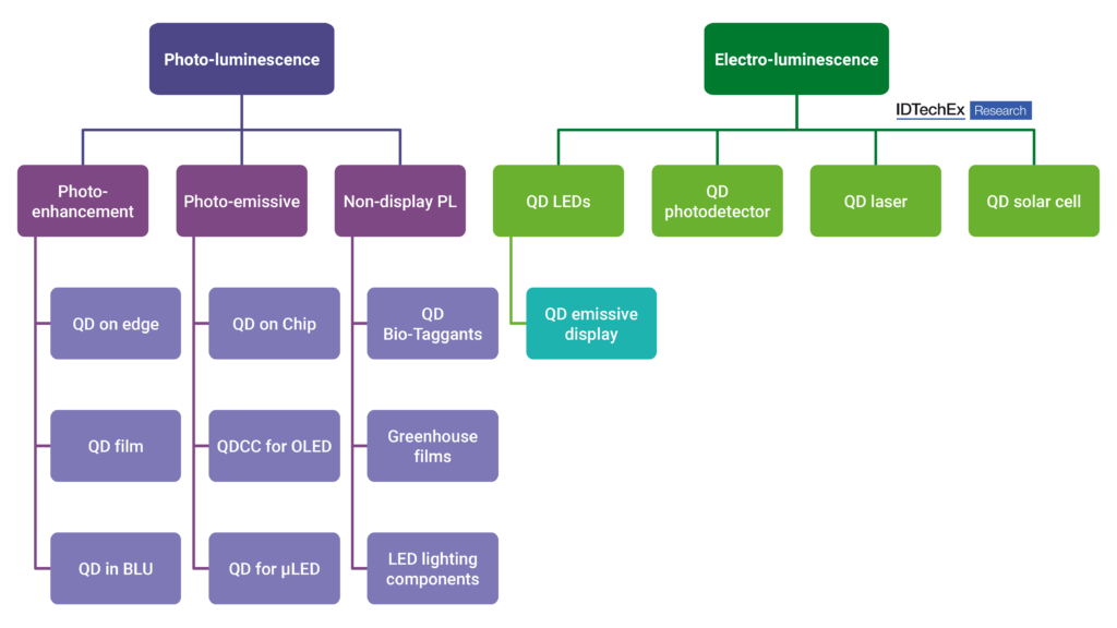
QDs were first discovered in 1980. They are semiconductor nanocrystals in the range of 2-10 nanometers (10-50 atoms) with size-tunable features. They exhibit quantum confinement effects due to their nanoscale dimensions, leading to remarkable optical and electrical characteristics. Both QD’s photoluminescent and electroluminescent features can be potentially applied in various applications with different levels of commercial readiness. Quantum dot features can be adjusted by particle size, material, and composition. QD materials such as Cd-based, In-based, PbS, perovskites, as well as emerging CuInS2, InAs, and ZnTeSe QDs have varied bandgap and thus absorption and emission spectra. This fine-tuning ability has resulted in quantum dots’ significant application potential, notably in displays, image sensors, photovoltaics, lighting, and various other use cases.
QDs are well known for their existing adoption in display applications. It is an emerging application to have QDs applied in image sensors, which are found in digital cameras, smartphones, and countless other devices, responsible for capturing and converting light into electronic signals that ultimately form images.
As the most widely used semiconductor material, silicon is an excellent choice for visible photodetectors. However, even longer wavelengths, such as near-infrared (NIR) or short-wave infrared (SWIR), may be required depending on the application. For NIR and SWIR sensing, especially above 1100nm, which are beyond silicon’s ability, silicon Read-Out Integrated Circuit (ROIC) is still utilized while alternative semiconductors need to be pursued for the photodetectors. The combination of the silicon ROIC and photodetector with heterogeneous materials can be achievable by three possible routes.
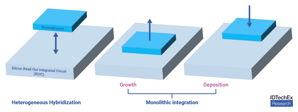
The incumbent III-V image sensor is fabricated by the so-called “heterogeneous hybridization” process, which applies to examples including indium gallium arsenide (InGaAs) and HgCdTe, etc. The alternative fabrication method is via monolithic growth of photodetector (such as germanium) on silicon ROIC.
QD and other solution processible materials can overcome the integration challenge of inorganic photodetector systems such as GaAs. This is because they can be applied directly onto the ROIC circuit via monolithic deposition.
Lead sulfide (PbS) QDs offer the advantage of tunability across an extensive spectrum of wavelengths, making them suitable for NIR or SWIR sensing applications. An intriguing possibility arises as they can be combined with a silicon ROIC to form a hybrid QD-Si NIR/SWIR image sensor. In this case, the sensing element can be arranged as a photodiode, photoconductor, or phototransistor.
This innovative integration presents a potential pathway towards achieving high-resolution small-pixel silicon-based NIR/SWIR sensors, eliminating the necessity for expensive and complicated heterogeneous hybridization of InGaAs sensors with Si ROIC. The low-cost hybrid QD-based image sensors can not only target applications traditionally realized by InGaAs SWIR image sensors but also help to reach new applications.
With the first generation of products already on the market and giants also getting involved in this area, the promise of this technology remains strong. This report explores hybrid QD-Si image sensors that can simultaneously achieve high resolution, low pixel pitch, and global shutter with potentially low costs. Technology analysis and player introductions are provided as well.
IDTechEx Research has been deeply engaged in the exploration of quantum dot technologies and markets since 2013. Throughout this period, IDTechEx has maintained a steadfast commitment to staying at the forefront of the latest research advancements and market trends. This has been achieved through an extensive interview program, direct interactions with companies, and active participation in relevant conferences and events.
Furthermore, IDTechEx Research has engaged closely with many of its clients, enabling a comprehensive grasp of their requirements. This collaboration has facilitated the provision of valuable insights into both the technological landscape and the dynamics of the market. Countless clients have benefited from this engagement, receiving strategic guidance for navigating the complexities of quantum dot technology innovation and commercialization.
Drawing from over two decades of experience in the analysis of advanced electronic materials and devices, IDTechEx Research has refined its expertise in evaluating emerging technologies. This extensive history provides a vantage point from which to understand the trajectories of various technologies, encompassing both their successes and setbacks.
This gives IDTechEx a uniquely experienced eye when it comes to analyzing emerging electronic material technologies. This is crucial because it helps us establish a realistic market and technology roadmap that reflects the true potential of the technology based on its intrinsic characteristics and the true level of technical and commercial challenges that it faces.


 combined with superior switching performance")


