


With IoT nodes and wearable devices shrinking, designers need to make maximum use of their microcontroller’s on-board memory to minimize board space, power, and cost. However, sometimes memory expansion cannot be avoided. Instead of defaulting to a 32-bit controller’s bus structure, designers should consider HyperBus, a high-speed, 333 Mbit/s, 8-bit, double data rate (DDR) interface for both address and data.
As much as designers try to avoid expansion, it’s often necessary due to increased memory requirements during development. Or, the developers are simply future-proofing the design by anticipating future expansion needs.
With HyperBus, microcontrollers can support external flash and RAM on the same bus, versus the 16-bit data and 16-bit address bus and associated control pins of a typical 32-bit interface. It works with any memory device that has a HyperBus interface port, and is an effective, easy-to-use interface for low pin count memory expansion in space-constrained applications.
Although the operation of the bus is transparent to firmware, it’s important that developers new to HyperBus familiarize themselves with the operation of the high-speed bus signals to ensure a robust design. This article will first describe the operation of HyperBus. It will then introduce microcontrollers that incorporate the interface, and show users how to go about applying it effectively and testing their design.
HyperBus explained
As mentioned, HyperBus uses a high-speed 8-bit DDR interface for both address and data. In addition, it uses a differential clock, a read/write latch signal, and a chip select for each memory device. HyperBus supports external flash and RAM on the same bus, and works with any microcontroller with a HyperBus compatible peripheral interface.
HyperBus is set up as a master/slave interface, where one host master interfaces to one or more slave memory devices on the bus. HyperBus flash memory devices are referred to as HyperFlash™, and HyperBus DRAM memory devices are referred to as HyperRAM™.
The bus uses a differential clock with signals designated CK and CK#. As HyperBus is a DDR interface, data is transferred on both rising and falling clock edges. The clock is driven only by the master, and its frequency may not exceed the rated clock frequency of the slowest HyperBus memory on the bus.
The bidirectional 8-bit bus is designated DQ[0-7] and transfers address, data, and commands between the master and slave devices. A bidirectional read/write data strobe signal, designated RWDS, is used to latch data. RWDS is controlled by whatever device is reading data, so if the microcontroller host is writing data to HyperRAM, the HyperRAM controls the RWDS signal. The data being read on DQ[0-7] is aligned with both edges of the clock.
Each slave device is selected using an active low chip select, designated CS0#, CS1#, CS2#, etc. Only one chip select may be active at any time. All bus transactions are initiated with the designated chip select transitioning from high to low. All bus transactions are terminated with the designated chip select transitioning from low to high. Developers must insure that one chip select is active at any time. Failure to do so may result in more than one HyperBus slave device driving RWDS at the same time, which can result in corruption of data.
An active low hardware reset signal, designated RESET#, is driven by the master. When pulled low, it resets the state of any external HyperBus memory devices connected to the signal. This includes resetting the memory device’s internal configuration registers. However, it does not affect the state of the internal memory of the HyperBus memory devices. On most HyperBus master microcontroller interfaces, RESET# is not part of the HyperBus peripheral but is instead a general I/O pin. HyperBus slave devices have a weak pullup on the RESET# pin, so if it is left floating it is pulled to a high state.
Any HyperBus-compatible peripheral on a microcontroller must conform to the HyperBus specification. A good example of a HyperBus-compatible microcontroller is the STM32L4R9 Arm Cortex-M4F from STMicroelectronics (Figure 1). The STM32L4R9 has 2 Mbytes of internal flash memory, and 640 Kbytes of SRAM. It has a wide variety of peripherals, including two OctoSPI interfaces that can be configured as HyperBus interfaces.
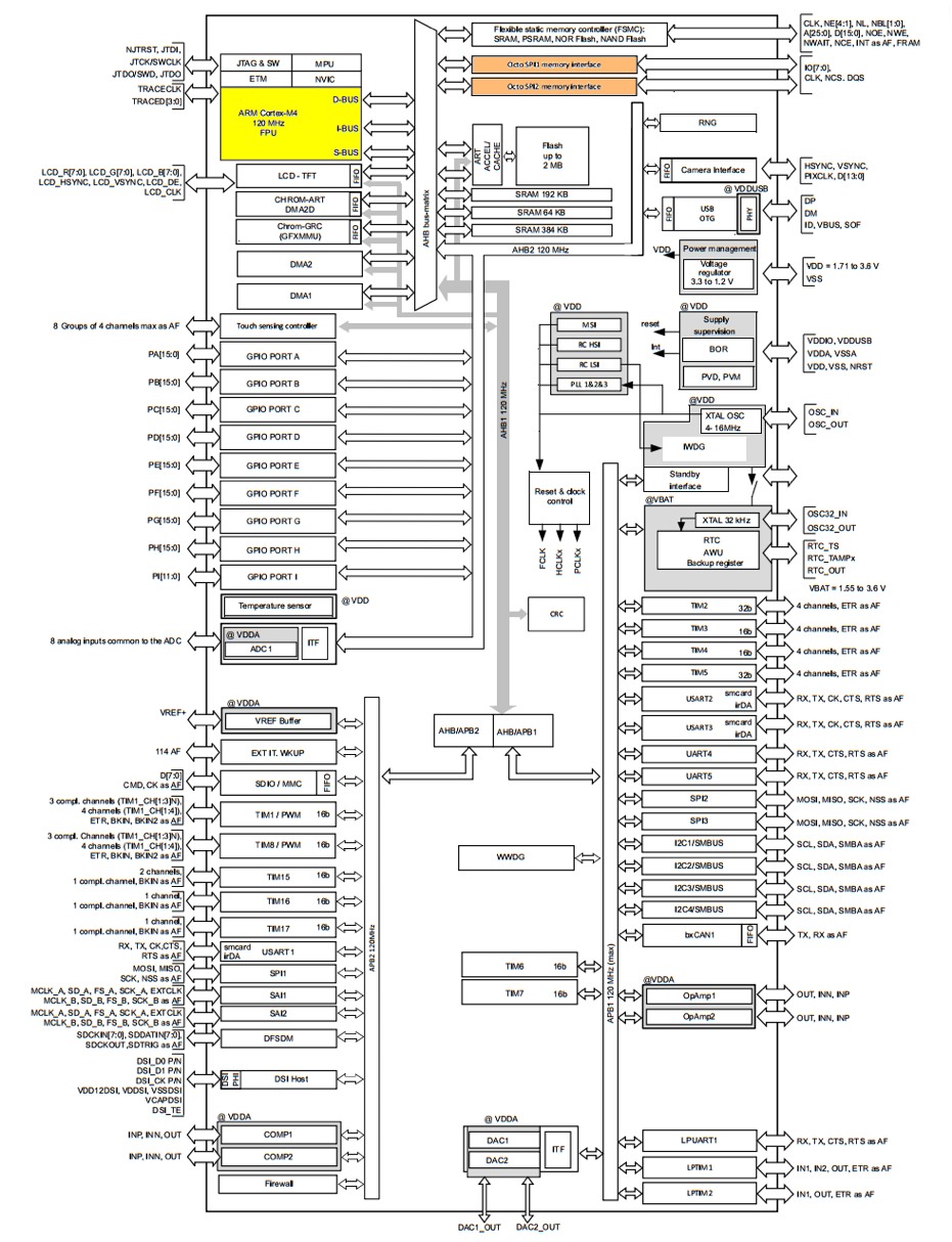
The STM32L4R9 accesses the HyperBus external memory addresses as memory mapped into the microcontroller’s AHB bus address space, so reads and writes to external memory are accessed by the core in the same way as internal memory. Once the external memory devices are configured, operation of the HyperBus is transparent to the core.
HyperBus memories are all 16-bit wide memories, so all accesses from the STM32L4R9 must be on 16-bit memory boundaries. Data accesses from the STM32L4R9 master can be 16-bit or 32-bit, and must also be on aligned boundaries.
A typical read or write transaction on the HyperBus consists of a sequential series of 16-bit, one clock cycle data transfers via two corresponding 8-bit wide, one-half clock cycle data transfers, one on each single-ended clock edge or differential clock crossing. Read and write transactions always transfer full 16-bit words of data. Read data words always contain two valid bytes. Write data words may have one or both bytes masked to prevent writing of individual bytes within a write burst. Byte transfers are not supported in the HyperBus protocol, nor does it support bit operations such as bit-banding.
Each HyperBus-compatible port on the STM32L4R9 has a dedicated 256 Mbytes of memory-mapped address space, mapped as follows:
HyperBus1 (OctoSPI1) 0x90000000 to 0x9FFFFFFF
HyperBus2 (OctoSPI2) 0x70000000 to 0x7FFFFFFF
The internal address of the HyperFlash or HyperRAM memory device being accessed is offset from the base memory address of the above location. For example, if the STM32F4L9 reads from memory location 0x90000047, it reads back the value stored in the memory device accessed on HyperBus1 in memory location 0x0047.
Cypress Semiconductor developed the HyperBus specification, and also has a product line of HyperBus memories. The Cypress S26KS512SDPBHI020 64 MB x 8 HyperFlash Memory can easily interface to one of the OctoSPI ports. It supports wrapped burst accesses of up to 32 16-bit words. With a maximum 166.6 MHz clock rate, the S26KS512 HyperFlash supports the full 333 Mbytes/s sustained read rate. At the OctoSPI maximum clock of 60 MHz, the STM32L4R9 can read any external HyperBus memory at 120 Mbytes/s, maximum.
The STM32L4R9 can execute code directly out of this flash memory if the HyperFlash is accessed through the Cortex-M4 system bus. When used for code memory, the OctoSPI supports eXecute In Place (XIP) with an integrated prefetch buffer that loads the next memory address from the external memory.
The Cypress Semiconductor S27KS0641DPBHI020 8 MB x 8 HyperRAM memory is a self-refreshed DRAM that can expand the STM32L4R9 data memory. It supports wrapped burst accesses of up to 64 16-bit words. The S27KS0641 HyperRAM also supports up to 333 Mbytes/sec sustained read rate and can be read by the STM32L4R9 at a maximum 120 Mbytes/s.
Interfacing to HyperBus memories
The STM32L4R9 has two HyperBus-compatible ports, and each can separately interface to HyperRAM and HyperFlash external memory devices (Figure 2). The RESET# signal is optional and so is not shown in the figure. With both the Cypress HyperFlash and HyperRAM, the STM32L4R9 can easily extend its internal memory with minimal impact on pc board size and design complexity.
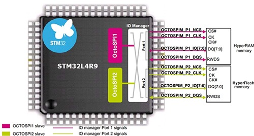
The most important signals for layout are DQ[0-7] and RWDS. For best performance, these signals should have the shortest length possible on the pc board between the microcontroller and the memory.
The differential clock signals CK and CK# should be next to each other with constant spacing between them for the length of the signals. If possible, shield CK and CK# with VSS guard traces to minimize EMI. To minimize impedance mismatch, break out all signals on the top layer of the pc board, with a solid VSS layer underneath.
For the developer new to HyperBus, it is a good idea to add probe test points. For DQ[0-7] and RWDS, test points should be at both the STM32L4R9 microcontroller and at the memory device. When the STM32L4R9 is writing, it’s good practice to look at the test points nearest the memory device. When the STM32L4R9 is reading, look at the test points nearest the STM32L4R9. For CK, CK#, and CS, put the test points nearer to the memory device.
Because of the high clock frequencies involved with the DDR interface, it is important that the voltage supply to the STM32L4R9 and the memory devices be as clean as possible. A noisy supply will affect signal timing and can cause bus transfer errors, so the use of decoupling capacitors is recommended. HyperBus memory devices have a separate power and ground for the I/O pins, and 1 microfarad (µF) and 0.1 µF capacitors on the top or bottom layer should be added to the I/O power VCCQ.
Firmware access to HyperBus
HyperBus memory devices have on-chip registers used to set options and timings for the device. HyperBus refers to these as Configuration Registers (CRs). All HyperRAM devices have internal CRs that allow setting certain operational characteristics. For the HyperRAM S27KS0641, firmware can configure its low-power modes, wrapped burst length, wrapped burst type, R/W timing parameters, and the output drive strength on the external 8-bit data bus.
HyperFlash does not have CRs but does have status registers. The S26KS512 HyperFlash has three status registers. It supports internal error correction code (ECC) for validating write operations and has an ECC status register to indicate write errors. Another register contains the address of any ECC errors. A third register counts the ECC corrections and uncorrectable errors. All of these registers are read-only.
HyperBus transactions support two types of memory operations. The first is reading or writing to external memory. The second is reading or writing to CRs or reading status registers.
Once the STM32L4L9 OctoSPI is configured as a HyperBus port, the core can access memory like any other memory-mapped location. Every read or write operation in the memory-mapped HyperBus space initiates a transaction between the microcontroller and the external memory. Each HyperBus transaction begins with the microcontroller sending three 16-bit words with Command/Address instructions to the external memory device. The Command/Address sequence tells the external memory device whether the operation is a read or write, if memory space or configuration registers are being addressed, if the transaction is a wrapped or linear burst transaction, and provides the target address row and column. While this is all transparent to the microcontroller with operational firmware, the Command/Address sequence is important during debug.
Getting started with HyperBus
Once the developer understands the HyperBus protocol, it is recommended that some experimental programming be performed with an evaluation board, especially if the developer is new to the interface. The STMicroelectronics STM32L4R9I-EVAL evaluation board for the STM32L4R9 microcontroller is a good starting point (Figure 3). The HyperRAM memory device is circled in red, with the device’s test points located on the header connector to the right.
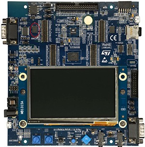
The STM32L4R9I-EVAL has a wide range of features, including a camera interface, two MEMS microphones, a joystick, and a 4.3 inch, 480 x 272 pixel, color TFT LCD display. The evaluation board supports the OctoSPI interface and has a IS66WVH8M8BLL 64 Mbit HyperRAM device from ISSI soldered to the pc board.
Conclusion
The HyperBus protocol is an appropriate, easy-to-use interface for low pin count memory expansion of space-critical applications. Although the operation of the bus is transparent to firmware, it’s important that the developer new to HyperBus familiarize themselves with the operation of the high speed bus signals to insure a robust design.


 combined with superior switching performance")


