


As all electronic systems require some kind of power, power supplies are well characterized and understood. Still, power supply design and selection continues to challenge engineers due to the trend toward smaller size, higher efficiency, higher reliability, and greater power integrity in applications from mobile devices to line powered hardware.
With high-speed data communications systems like 5G emerging, the timing and noise margin requirements become quite extreme.
To solve the problem of efficient and reliable power delivery in a small form factor, power supply designers are using switch mode power supplies (SMPS) with a flyback topology. This topology, useful to power levels of up to 150 Watts, offers designs with low component count for small size and low cost. It also offers input/output isolation, and good efficiency.
This article will discuss the operation of switch mode power supplies and explore briefly the make vs. buy decision process for power supplies. It will also investigate the design of a single output supply utilizing flyback topology and provide a sample design using readily available parts and components.
Switch mode power supplies
An SMPS, or switcher, is a power source that uses a switching regulator to maintain stable output voltage(s) from an AC or DC source. The switching regulator uses one or more semiconductor devices such as a bipolar junction transistor, MOSFET, or IGBT switching between ‘On’ and ‘Off’ states to maintain output voltage regulation. These devices can operate with fixed ‘On’ time and variable frequency, or more commonly, at a fixed frequency and variable duty cycle. High efficiency results from the low power dissipation of the switching device when it is either ‘On’ or ‘Off’. The device dissipates power only during the transitions between states. Also, because the switching frequency is generally in the tens of kilohertz, transformers, inductors, and capacitors can be much smaller, giving high volumetric efficiency.
The advantages of the SMPS are countered by the potential for electromagnetic interference (EMI). This is due to the switching transients and can be ameliorated by careful component selection, layout, and shielding. As a result, the SMPS’s advantages far exceed its drawbacks making them the most commonly used power supply, with linear supplies relegated to only the most sensitive electronic applications.
SMPS topology
SMPS can be realized in a large variety of circuit designs or topologies. There are over a dozen commonly used topologies (Table 1).
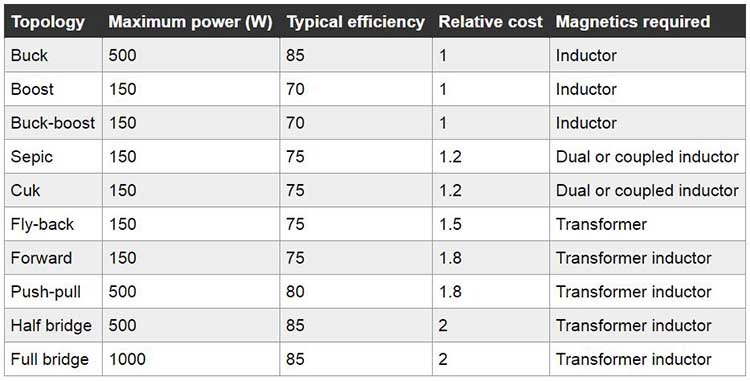
Table 1: The 10 most commonly used switch mode power supply topologies (Data source: Digi-Key Electronics)
Flyback topology
The flyback converter is the most commonly used SMPS circuit (Figure 1).
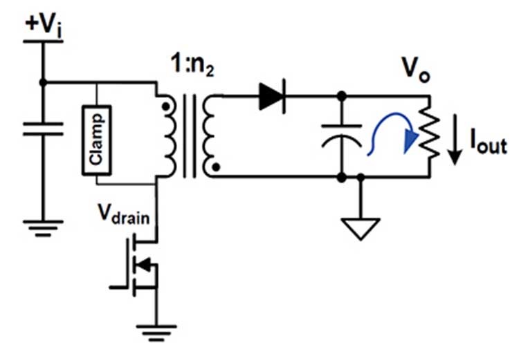
Figure 1: Functional diagram of a flyback converter using a single MOSFET switch and a flyback transformer. (Image source: Digi-Key Electronics)
The chief advantage of the flyback topology is its simplicity. At any given power level it has the lowest component count of the SMPS topologies. The supply can be powered from a DC or an AC source. When configured to operate from the AC line (mains), the line is generally full wave rectified. The input source (Vi) is DC.
The heart of the circuit is the flyback transformer. Unlike conventional transformer windings the primary and secondary winding of the flyback transformer do not carry current at the same time. This is due to the winding phase being reversed, as indicated by the dot notation on the windings and the series diode on the secondary side.
The use of the flyback transformer offers several benefits. The first is that the primary and secondary sides of the supply are electrically isolated. Isolation reduces the coupling of transients from the primary side, removes ground loops, and offers greater flexibility in the supply’s output polarity.
The transformer allows multiple output voltages to be generated in the supply. Additional windings for each voltage are added to the transformer. Regulation is based on only a single output, and the secondary outputs are generally regulated locally.
The circuit operation begins with the switch (such as a MOSFET) being turned on (Figure 2).
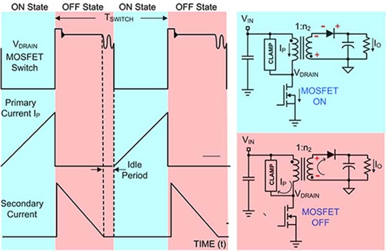
Figure 2: The operation of the flyback supply showing the principle waveforms for each of the two operating modes. (Image source: Digi-Key Electronics)
When the switch is on, VDRAIN is near zero volts and the current, IP, flows through the primary winding of the transformer. Energy is stored in the magnetizing inductance of the transformer. This current rises linearly with time. On the secondary side the series diode is reversed biased and no current flows in the secondary. Energy stored in the output capacitor supplies current to the output.
When the MOSFET switch is turned off, the energy stored in the transformer is output through the diode into the output capacitor and the output load. The secondary current starts at a high value and ramps down linearly. If the secondary current drops to zero before the switch is again turned on, the supply is referred to as a discontinuous current mode (DCM) supply. If the secondary current does not fall to zero, then the supply is called a continuous current mode (CCM) supply. As the energy stored in the inductor is fully discharged on each switching cycle, the DCM supply can use a smaller transformer. Additionally, the supply is generally more stable and produces lower EMI.
The energy stored in the transformer’s leakage inductance flows in the primary when the switch turns off and is absorbed by the input clamp or ‘snubber’ circuit, the function of which is to protect the semiconductor switch from high inductive voltages. Power is dissipated only during the switch’s transitions between the ‘ON’ and ‘OFF’ states (Figure 3).
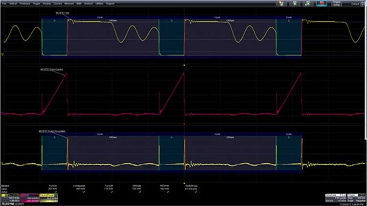
Figure 3: Measurement of a flyback supply showing the voltage and current waveforms at the MOSFET switch, along with the instantaneous power dissipation. (Image source: Digi-Key Electronics)
The top trace in Figure 3 is the voltage across the MOSFET switch in a flyback power supply. The colored overlays indicate the state of the MOSFET. The blue overlay indicates that the device is conducting, while the red areas indicate that the device is OFF. The center trace is the current through the device. The bottom trace shows the instantaneous power computed as the product of applied voltage and resultant current. Observe that power dissipation is most significant during the switching transitions. The readouts below the trace display show (left to right): power losses during turn on, conduction, turn off, during the off state, and the sum power losses for all zones.
Controller/regulators
The switching device, such as the MOSFET in the diagram (Figure 2 again), is driven by a controller or switch mode regulator. In most cases the controller applies a pulse width modulated (PWM) waveform to the control element of the switch, which for MOSFETs is the gate. The output of the supply is coupled back to the controller, which varies the duty cycle of the gate drive signal to maintain a constant output voltage. As such, the controller forms a closed-loop control system about the flyback converter.
Controllers may also handle several auxiliary functions, such as protecting the supply from overloads, over voltage, or low line conditions. It may also manage the startup of the supply to insure a well-controlled (‘soft’) startup, minimizing initial current and voltage transients.
SMPS design
Several semiconductor component suppliers offer design tools to help design switch mode power supplies, such as WEBENCH Power Designer from Texas Instruments (Figure 4).
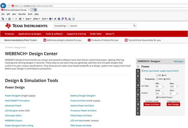
Figure 4: The opening page of the Texas Instruments WEBENCH Power Design Center shows the basic specification for an SMPS design of a 25 Watt 5 volt flyback power supply. (Image source: Digi-Key Electronics)
The design starts with user entered power specifications of supply voltage range, desired output voltage, and current. In this case the desired design was for a 5 volt, 5 amp supply operating from AC with an isolated topology. For more complex, multi-output supplies, there is an advanced Power Architect design tool.
From this point, the software initiates a series of designs and prompts for the user’s choice of the controller. The user can review each design to see the schematic, bill of material (BOM) costs, efficiency, and a dozen related circuit specifications.
In this example the Texas Instruments UCC28740 flyback converter was selected and the design schematic was displayed (Figure 5).
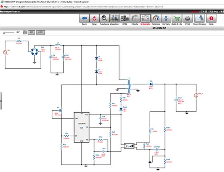
Figure 5: Schematic of the 25 watt AC SMPS using optically isolated feedback suggested by WEBENCH. (Image source: Digi-Key Electronics)
Pointing at any component on the schematic brings up a detailed part description and the opportunity to select an alternative component. The controller (U1) receives feedback from the output via a CEL PS2811-1-F3-A optoisolator. This method of feedback maintains the electrical isolation between the primary and secondary sections of the circuit. The controller provides the PWM drive signal to the power switch M1, STMicroelectronics’ STB21N90K5 900 volt, 18.5 amp, MOSFET. The design tool also helps select or design the flyback transformer.
A design summary page provides an overview of the key design elements (Figure 6).
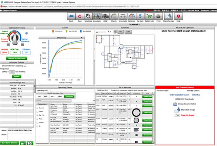
Figure 6: The design summary consolidates all the elements of the suggested design. (Image source: Digi-Key Electronics)
The optimizer Tuning section allows the user to optimize the design for lowest BOM cost, smallest footprint, or the highest efficiency. Using this tool permits inexperienced designers to gain experience by reviewing multiple designs and seeing the effects component changes produce.
Make or buy?
There is no doubt that unless an engineer has experience with SMPSs there will be a learning curve. If time to market is a big concern, then it is best to buy a standard supply or contract for a custom power supply design. Having the time and the technical staff, especially if multiple projects need supplies, then designing a supply would be worthwhile. That said, repeated exposure to SMPS design will add needed expertise to the design staff.
Conclusion
Switch mode power supplies offer high efficiency and small size. For power levels under 150 watts, the flyback topology supplies pose the advantages of multiple outputs, low component count and line isolation.
About this author

Art Pini Arthur (Art) Pini is a contributing author at Digi-Key Electronics. He has a Bachelor of Electrical Engineering degree from City College of New York and a Master of Electrical Engineering degree from the City University of New York. He has over 50 years experience in electronics and has worked in key engineering and marketing roles at Teledyne LeCroy, Summation, Wavetek, and Nicolet Scientific. He has interests in measurement technology and extensive experience with oscilloscopes, spectrum analyzers, arbitrary waveform generators, digitizers, and power meters.


 combined with superior switching performance")


