2D Materials
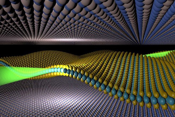
In our daily life, we always come across 3D materials but scientists and engineers are exploring 0D, 1D and 2D materials for their exotic properties. Two-dimensional (2D) materials are a class of nanomaterials that have two dimensions (XY plane) outside of the nanometric size range and atomic-scale thicknesses (Z dimension). The first well-known 2D material is graphene consisting of a single layer of carbon atoms arranged in a hexagonal lattice. To compare with 0D material (fullerene) and 1D material (carbon nanotube), the researches related to 2D material (graphene) have grown up quickly over other carbon allotropes. However, it is not only 2D graphene that has been widely applied in a large variety of potential applications but also other 2D materials such as tungsten disulfide, molybdenum disulfide, and silicon nitride open up new opportunities for the future devices. MXenes are the newest two-dimensional (2D) material family of layered transition metal carbides, nitrides and carbonitrides. Some examples of new 2D materials are transition metal dichalcogenides (TMDs), mono-natural 2D sheets, carbides, and nitride-based materials. Although a tremendous number of earlier studies focus on graphene and its derivatives, other emerging elemental 2D materials, such as borophene, silicene, black phosphorene, antimonene, tellurene, bismuthene and arsenene, are attracting increasing research interest in electronics and optoelectronics, as well as various electronic and computer devices. Similar to the structure of graphene, two-dimensional semiconductors are its two-dimensional and isostructural counterparts based on the typical layer-structured semiconductors, such as boron nitride (h-BN) and transition metal dichalcogenides (e.g. MoS2 and WS2), whose layers are bound by weak van der Waals forces.
Two-dimensional materials, which are only a few atoms thick, can exhibit some incredible properties, such as the ability to carry electric charge extremely efficiently, which could boost the performance of next-generation electronic devices. But integrating 2D materials into devices and systems like computer chips is notoriously difficult. These ultrathin structures can be damaged by conventional fabrication techniques, which often rely on the use of chemicals, high temperatures, or destructive processes like etching. The challenges were securing single crystallinity at the wafer-scale; avoiding irregular thickness during growth at the wafer-scale; and vertical heterostructures at the wafer-scale. Accordingly, 3D materials undergo a roughening and smoothing process to achieve an even surface. However, 2D materials do not permit this process, resulting in an uneven surface that makes large-scale, high-quality, uniform 2D materials impossible to achieve. Another technical breakthrough was demonstrated by the researchers by layer-by-layer growth of single-domain heterojunction TMDs at the wafer-scale, or a large scale. They employed a variety of chemical compound substrates to limit the growth of the nuclei. These substrates developed a physical barrier that hindered the establishment of lateral-epitaxy and promoted vertical growth. Developing high-quality 2D Materials that power next-generation electronics, scientists have been looking for materials that can substitute silicon in electronics and offer improved performance, lower power consumption, and scalability. 2D materials provide exceptional performance benefits over existing technologies at the device level. They also carry the promise of easy integration with silicon CMOS technology. This makes them prime candidates for substantially expanding the functionality of silicon chips, also referred to as “CMOS + X”. Scientists and technologists are confident that 2D materials will increasingly become such an X-factor in future integrated products. The bottleneck towards 2D material-based heterogeneous electronics is reaching the required manufacturing readiness levels, which may be different depending on the targeted application.
Characteristics of 2D materials
Graphene and two-dimensional materials remain an active field of research in science and engineering over 15 years after the first reports of 2D materials. The vast amount of available data and the high performance of device demonstrators leave little doubt about the potential of 2D materials for applications in electronics, photonics and sensing. The key highlights of 2D materials are:
- Atomically clean interfaces: The new stamp design has enabled the creation of atomically clean interfaces between stacked 2D materials over extended areas, a significant improvement over existing technique.
- Reduced strain inhomogeneity: The rigidity provided by the new stamp design has been shown to greatly reduce strain inhomogeneity in assembled stacks.
- Scalability: The team has demonstrated clean transfer of mm-scale areas of 2D materials, paving the way for the use of these materials in next-generation electronic devices.
Present status of development
Researchers at the University of Manchester have made a breakthrough in the transfer of 2D crystals, paving the way for their commercialisation in next-generation electronics. This ground-breaking technique utilises a fully inorganic stamp to create the cleanest and most uniform 2D material stacks to date. The research team employed the inorganic stamp to precisely ‘pick and place’ 2D crystals into van der Waals heterostructures of up to 8 individual layers within an ultra-high vacuum environment. This advancement resulted in atomically clean interfaces over extended areas, a significant leap forward compared to existing techniques and a crucial step towards the commercialisation of 2D material-based electronic devices. Moreover, the rigidity of the new stamp design effectively minimised strain inhomogeneity in assembled stacks. The team observed a remarkable decrease in local variation – over an order of magnitude – at ‘twisted’ interfaces, when compared to current state-of-the-art assemblies. The precise stacking of individual 2D materials in defined sequences holds the potential to engineer designer crystals at the atomic level, with novel hybrid properties. While numerous techniques have been developed to transfer individual layers, almost all rely on organic polymer membranes or stamps for mechanical support during the transition from their original substrates to the target ones. Unfortunately, this reliance on organic materials inevitably introduces 2D material surface contamination, even in meticulously controlled cleanroom environments. In many cases, surface contaminants trapped between 2D material layers will spontaneously segregate into isolated bubbles separated by atomically clean areas. This segregation has allowed to explore the unique properties of atomically perfect stacks. However, the clean areas between contaminant bubbles are generally confined to tens of micrometres for simple stacks, with even smaller areas for more complex structures involving additional layers and interfaces.
This ubiquitous transfer-induced contamination, along with the variable strain introduced during the transfer process, has been the primary obstacle hindering the development of industrially viable electronic components based on 2D materials. The polymeric support used in conventional techniques acts as both a source of nanoscale contamination and an impediment to efforts to eliminate pre-existing and ambient contaminants. For instance, adsorbed contamination becomes more mobile at high temperatures and may be entirely desorbed, but polymers cannot typically withstand temperatures above a few hundred degrees. Additionally, polymers are incompatible with many liquid cleaning agents and tend to outgas under vacuum conditions. To overcome these limitations, we devised an alternative hybrid stamp, comprising a flexible silicon nitride membrane for mechanical support and an ultrathin metal layer as a sticky ‘glue’ for picking up the 2D crystals. Using the metal layer, we can carefully pick up a single 2D material and then sequentially ‘stamp’ its atomically flat lower surface onto additional crystals. The van der Waals forces at this perfect interface cause adherence of these crystals, enabling us to construct flawless stacks of up to 8 layers. After successfully demonstrating the technique using microscopic flakes mechanically exfoliated from crystals using the ‘sticky tape’ method, the team scaled up the ultraclean transfer process to handle materials grown from the gas phase at larger sizes, achieving clean transfer of mm-scale areas. The ability to work with these ‘grown’ 2D materials is crucial for their scalability and potential applications in next-generation electronic devices.
Indeed, over a dozen 2D materials have been already discovered that exhibit programmable resistive switching – the fundamental property for building devices (memristors) that can be used to mimic the behavior of synapses and neurons. While many fundamental aspects still need to be understood, the first memristors based on 2D materials have shown competitive performance as well as a wide range of desirable non-computing functions, such as un-clonability and radio-frequency switching for communication systems. Another future field where 2D materials can play a major role are quantum technologies. There is consistent evidence that 2D materials have a large potential for solid-state quantum computing, as well as for quantum communications and for novel quantum-sensing schemes. Further, the flexibility offered by the 2D-platform might offer some major advantages in the middle to long term, and allow overcoming some of the roadblocks encountered by other platforms, such as spin to photon coupling.


