


Abstract
A 50W switching supply suitable for telecom applications is described. The supply, a high-frequency forward converter, provides an isolated 5V @ 10A with 1% line and load regulation. A buck converter topology is selected after considering flyback and buck converters. The MAX5003 control IC is selected; its features and circuit are described. Important waveforms are shown and discussed; the power transformer is detailed; input, output, and feedback circuits are discussed. Performance is detailed and preferred PCB layout is provided.
Also see:
- MAX5003 QuickView Data Sheet
- MAX5003-50WEVKIT
- MAX5003EVKIT
- Design and simulate isolated power supplies with free MAX5003 Isolated Power Supply Design Software.
This 50W, isolated power-supply design can be used to replace purchased supplies with minimal additional engineering effort. The advantages of such an approach also include the accommodation of custom footprint and substantially lower cost.
The Challenge
Power supplies are often an afterthought. Purchased power-supply “bricks” are a quick solution, but with significant disadvantages, such as size, heat-sink and airflow requirements, long lead times, limited configurations, and higher overall costs. An in-house design usually fits product requirements better, but may not seem possible without a dedicated group of power-supply design engineers.
“Off-the-Shelf” Design
A few semiconductor companies are providing reference designs that can greatly streamline power-supply design and bring custom supply designs within reach. An “off-the-shelf design” makes it possible to quickly produce a supply that is smaller and simpler to integrate, performs better, and delivers much lower cost and superior time-to-market.
Telecom/Datacom/Server Power Supplies
A kind of power supply that is currently in great demand is the telecom, datacom type. Such power supplies are utilized in central offices, PBXs, and servers, and typically use an input voltage of 36V to 72V. Their typical output power levels range from about 10W to 100W or even higher. Important requirements for these power supplies are galvanic isolation between primary and secondary, high efficiency over a wide input-voltage range, and ruggedness. The design of such power supplies, however, is relatively complex due to the requirements of isolation.
50W Isolated Power Supply
Figure 1 shows a 50W “off-the-shelf-designed” power supply. This is an isolated power supply with a 5V regulated output. Table 1 summarizes some of the target specifications.
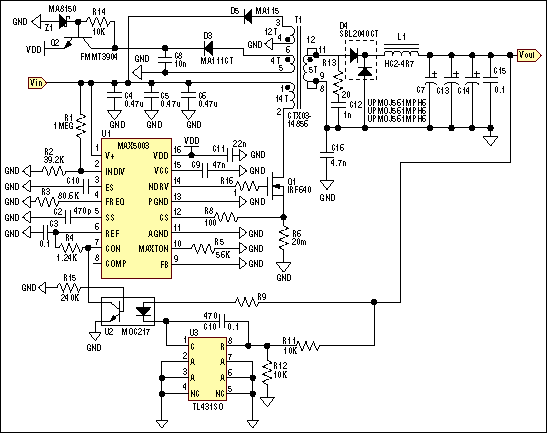
Table 1. Summary of Target Specifications
| Pout | 50W |
| Vin | +36V to +72V or |
| Vin | -36V to -72V |
| Vout | +5V |
| Iout | 10A |
| Initial Output-Voltage Set-Point Accuracy | ±3% |
| Output-Voltage Regulation | <1%, over line and load |
| Switching Frequency | 250kHz ±25% |
| Input-Output Isolation | 1500V for 1sec |
Power Circuit Topology
Among the several power topologies available, the single transistor forward topology offered the simplest lower-cost solution while providing very good efficiencies throughout the operating power range. This topology, however, requires a transformer reset winding that is connected to pins T1-3 and T1-4. The forward converter was chosen, because it offers higher power density and higher efficiency than a flyback converter at these power levels. Although first-order flyback topology schematics tend to look simpler, these converters are more difficult to deal with (see the brief comparison below). Transformer T1 provides the necessary isolation between primary and secondary, in this case 1500V. In addition, efficiency is improved by powering the control circuit in the primary (T1-5, T1-6 leads) after initial startup. A 250kHz switching frequency was selected to allow for minimization of the energy storage components, such as transformers.
Forward and Flyback Converters: A Comparison
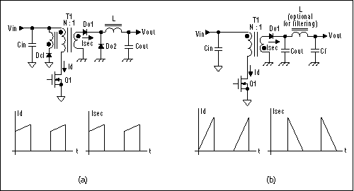
Figure 2a shows the power-stage configuration of a forward converter. Power transfer to the secondary-side circuit takes place when the power switch Q1 is turned on. Almost all forward supplies are operated in continuous conduction mode, which means that the inductor energy is not completely depleted before the start of the next cycle. The drain current Id looks rectangular with a slight pedestal. When Q1 turns off, Do1 reverse-biases, whereas Do2 forward-biases, carrying the entire inductor current. The reset winding that is connected to the cathode of Dcl allows for the recycling of the energy stored in the transformer core by returning it to the input source.
Figure 2b shows the power stage of a flyback converter. In this case, power transfer to the secondary takes place after Q1 has turned off. Energy stored in the transformer core is delivered to the load. Flyback converters tend to cost less for lower-power applications, because they don’t require an output inductor. A small filtering inductor is sometimes used, however, to reduce high-frequency spikes that are present at the output voltage. Flyback converters are often operated in discontinuous mode, which means that the energy stored in the transformer is transferred completely to the output before the start of the next cycle.
Control Circuit
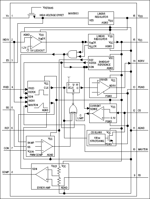
The primary-side control circuit is based on the MAX5003. A simplified block diagram of this IC is shown in Figure 3. The MAX5003 represents the next generation of power-supply controllers that integrate many functions that are necessary for the design of telecom power supplies. It contains a high-voltage startup circuit that speeds up the initial power-up process. It also has other abilities that ease the design of isolated, regulated, telecom power supplies, such as voltage feed-forward compensation. Voltage feed-forward is an important element of the design, because it helps to provide constant power-stage gain that results in more stable voltage control loops. It also significantly helps with input supply rejection by instantly responding to varying input voltages and correcting the duty cycle within a single cycle without the intervention of the slower-voltage control loop.
The following equations should help you understand the effect of feed-forward compensation. The large signal modulator and power-stage gains of a forward converter without feed-forward compensation are given in equations (1) and (2), respectively.
| (1) |
where d is the duty cycle, vc is the control voltage present at the input of the PWM comparator (pin 7), k1 is a constant, and sr is the slope of the internal modulating ramp.
| (2) |
where k2 is a constant, vout is the output voltage, and vin is the input voltage.
The combination of equations (1) and (2) results in equation (3), which is the known ideal gain expression for forward- and buck-type regulators. However, in this expression, it is seen that the power-stage gain vout/vc is dependent on the input voltage.
| (3) |
This dependence of the power-stage gain on the input voltage limits the attainable control-loop bandwidth in systems where the input voltage is subject to wide variations. Also, any fast perturbation on the input-voltage line directly affects the output voltage, as can be seen from equation (3). The only correction to such perturbation to keep the output voltage constant must come from changing vc, which entails the intervention of the relatively slow voltage error amplifier.
In a feed-forward compensated system, the slope of the regulating ramp is made inversely proportional to the input voltage, as given by equation (4):
| (4) |
By substituting equation (4) in equation (3), the constant gain expression of equation (5) is obtained:
| (5) |
It is clearly seen from equation (5) that the dependency of the output voltage on the input voltage has been completely eliminated, as virtually all input-voltage transients are rejected by the power circuit even without the intervention of the output-voltage control loop.
By using an external resistor, the switching frequency has been set to be 250kHz. This helps to minimize the size of the energy storage components without a big switching power loss penalty.
Forward converters with a reset winding (terminals 3 and 4 of the transformer) need to have their maximum duty cycle clamped to specific levels to avoid transformer-core saturation due to insufficient core reset. In general, the following condition must be met under all conditions to prevent transformer-core saturation:
| (6) |
where N12 and N34 are the number of turns of the main and reset windings. Written in simplified form, equation (6) sets the condition that must be met for the duty cycle:
| (7) |
The MAX5003 provides for the maximum-duty-cycle limit by programming the MAXTON pin with a single resistor, thus helping to meet the above condition for an optimized design.
Telecom-grade power supplies also require an undervoltage lockout function. This is used to disable the power supply if the input voltage “dips” lower than a preset voltage (less than 32V in most systems). The undervoltage lockout threshold of this power supply is set by the voltage divider R1/R2.
Startup Circuit
The MAX5003 controller contains an internal high-voltage preregulator that directly connects to the input voltage. Power is fed from the V+ pin into a depletion junction FET preregulator. The preregulator drops the input voltage to a level low enough to feed a first low-dropout regulator (Figure 3). The input to the LDO is brought out at the ES pin, where it is decoupled with a small ceramic capacitor. The output of the primary-side bias winding (T1-5 and T1-6) is rectified with D3 and applied to a voltage-level conditioning circuit comprised of R14, Q2, and Z1. This circuit limits the voltage to a safe level so that it can be applied to the VDD. The bias winding in this case operates in flyback mode, as opposed to the power stage that operates in forward mode. This eliminates the need for a filter inductor, reducing cost. Energy to the winding in the flyback mode is supplied by the energy stored in the magnetizing inductance of the transformer during the on time.
During initial startup, the first regulator generates the power for the VDD line, which is available externally through a corresponding pin. Forcing voltages at VDD above 10.75V disables the first LDO, turning off the high-voltage depletion FET, thus reducing power consumption by the IC especially at high input voltages. Following the VDD, the LDO is another regulator that drives VCC: It is the power bus for the internal logic, the analog circuitry, and the driver for the external power MOSFET. This regulator is needed because the VDD voltage level would be too high for the external N-channel MOSFET gate. The VCC regulator has a lockout line that shorts the N-channel MOSFET driver output to ground if the VCC LDO is not regulating. VCC feeds all circuits except the VCC lockout logic, the undervoltage lockout, and the power regulators.
Transformer
A key component in any isolated power supply is the power transformer. Critical specifications of the power transformer that have a direct impact on efficiency and reliability are the primary and the secondary winding DC and AC resistances, resulting in operating losses. The AC part of the losses comes from skin and proximity effects and, depending on the transformer (whether is gapped or not), from circulating eddy currents. The proximity effect is the consequence of magnetic fields that distort the current flow in nearby winding conductors. The winding configuration plays a big role in these losses.
Another key parameter is leakage inductance. Leakage inductance is a critical parasitic element that must be kept as low as possible to maximize power transfer to the secondary. Low leakage inductance also reduces losses in the primary. In this design, part of the leakage energy is dissipated across Q1. Figure 5 clearly shows the spike at the drain of Q1, briefly after turning off. A less critical parameter is magnetizing inductance. This is the inductance seen from the primary terminals 1 and 2 with all other terminals open-circuited. Table 2 gives the transformer specifications.
The following formula can be used to roughly calculate the energy stored in the leakage inductance and therefore dissipated in the MOSFET:
| (8) |
where Ip is the peak primary current when the MOSFET turns off and LLeak is the primary-side leakage inductance.
Table 2. Transformer Specifications
| Primary Turns (N1-2) | 14 |
| Secondary Turns (N8,9-11,12) | 5 |
| Bias-Winding Turns (N5-6) | 4 |
| Reset-Winding Turns (N3-4) | 12 |
| Magnetizing Inductance (N1-2) | 250µH |
| Leakage Inductance | <1µH |
| Hipot Secondary to Any Other Winding | 1500V for 1sec |
| Core Geometry | EFD20 |
| Core Material | High-frequency ferrite |
| Mounting | 12-pin surface-mount bobbin |
The circuit in Figure 1 shows the electrical diagram of the transformer. Of importance are the winding-phase relationships noted with the dots next to the winding terminals.
Output Circuit
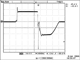
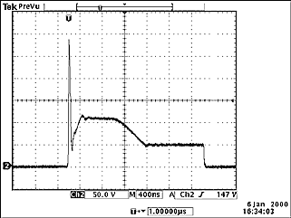
The output uses a low forward drop, dual Schottky diode, for high efficiency. This diode is rated to 20 amps with a 40V reverse breakdown voltage, adequate for this application. The total average current rectified by the diode is 10A, resulting in approximately 5.5W of power dissipation. The diode needs a heatsink capable of keeping the junction temperature at acceptable levels under worst-case ambient temperature conditions. Figure 4 shows the output voltage at the secondary of the transformer. Notice the negative-going spike on this waveform. The energy in this spike is small, and the diode is able to absorb this energy safely; in addition, the R/C network R13/C12 helps to reduce ringing at the secondary side.
Inductor L1 is capable of conducting 10A without significant losses. It is a 4.7µH high-current surface-mount type. Although it is rated for higher currents, the low series resistance helps to keep losses low. The ripple current is approximately 2.2A peak to peak. Thus, the inductor current becomes discontinuous with an output current of approximately 1.1A.
The output capacitors can be either tantalum or aluminum electrolytic types. There are three primary considerations when selecting these capacitors: allowable AC ripple-current handling, output-voltage ripple, and (as it will be seen later) control-loop stability. When using low-cost electrolytics, additional low-value ceramic capacitors can be used to further reduce switching noise spikes at the output terminals. In this circuit, the expected AC RMS current through the capacitors is in the order of 0.8A RMS; therefore, these capacitors should be sized to safely handle this level of ripple current.
Feedback Circuit
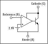
The two main elements of the voltage feedback circuit are the TL431 shunt regulator and the optocoupler MOC207. Figure 6 shows the internal block diagram for the TL431. Several manufacturers produce this part, and it comes in various grades of accuracy. The internal reference voltage of the shunt regulator is 2.5V typical. An external voltage divider is used, and it consists of R11/R12 for a 5V regulated output voltage. This feedback-circuit configuration is very common in switching power supplies and is used widely. However, its operation sometimes is misunderstood, resulting in potential pitfalls. This circuit has two feedback paths from the output. One path is through the shunt regulator, providing the low-frequency gain for good output-voltage regulation, whereas the second path is through the optocoupler itself to the cathode terminal of the shunt regulator. To visualize this latter loop, it suffices to replace the shunt regulator with a virtual constant voltage source.
In this arrangement, any increase in output voltage will result in a higher current flowing through the LED of the optocoupler, forcing the collector voltage of the coupled phototransistor to fall and thus reduce the duty cycle. This results in a negative feedback loop that has the tendency to keep the output voltage constant. Therefore, care must be exercised when trying to stabilize this loop. The easiest method and the one adopted in this design is to rely on the ESR of the output capacitors for proper compensation of this latter feedback path. However, this puts a constraint on the minimum value of the ESR. The following formula provides a good rule of thumb for the ESR:
| (9) |
Tolerances of ±30% for the ESR should be certainly adequate. It’s important to point out that by meeting equation (8) in an otherwise well-designed system, the phase margin at the unity gain crossover point of the control loop approaches 90 degrees for a excellent transient response.
Example:
| (10) |
Thus, in order to get the required ripple at the output, one or more capacitors may have to be paralleled. For a 50mV peak-to-peak voltage ripple at the output, four 330µF capacitors that have an ESR of 90mΩ each can be used.
The compensation capacitor around the shunt regulator in most cases is not very critical, and its value can be around 0.1µF. Much lower values should not be used for this capacitor, as they could reduce the overall phase margin of the control loop.
The feedback circuit is completed in the primary by connecting the collector of the phototransistor in U2 to the CON input of the MAX5003. Although the control IC contains an error amplifier, that amplifier is not used in this case. However, this amplifier is very useful for non-isolated applications and in cases where regulation is done through a biasing auxiliary winding connected to the primary side.
Input Circuit
The input circuit consisTs of three ceramic bypass capacitors, c4/c5/c6. When embedding the power supply to an actual system, it is advisable to use bulk storage capacitors. These capacitors must be sized so that they can safely handle the ripple currents present at the input of the converter.
| (11) |
where Ip is given by the following:
| (12) |
It should be noted that the worst-case ripple current through the input capacitor is around 50% duty cycle. For the circuit in Figure 1, the AC capacitor ripple current is 1.5A RMS. These capacitors should be placed very close to the input to avoid long traces from carrying high-frequency switching currents that can cause EMI problems. Additional input filtering may be necessary to meet applicable regulations.
Key Power-Supply Waveforms
Waveforms at key points of the circuit help explain the operation further. Figure 5 shows the drain source waveform of the switching FET. The initial spike is a result of the leakage inductance of the transformer. This is much lower at lower-output power levels. In this case, the FET absorbs the leakage energy.
Figure 7 shows the voltage pulse at the output of the secondary rectifier. This is a relatively clean waveform with minor leading- and trailing-edge spikes.
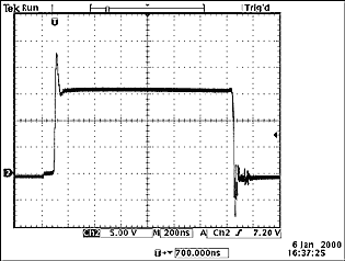
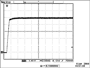
Figure 8 shows the well-behaved rise of the output voltage. The soft-start feature of the MAX5003 gradually increases the duty cycle, thus eliminating any potential overshoots during startup.
Power-Supply Performance
Key performance characteristics of the power supply include efficiency and output-voltage-regulation curves. Figure 9 shows the efficiency versus output power. The efficiency reaches 85% at about 25W of output power and stays relatively flat up to 50W. Even though the efficiency is very high, heatsinking is required for the power FET and output diodes. The diode will dissipate about 6W with a 10A output current, and the FET can be expected to dissipate about 3W to 4W. A slight airflow over the power supply will cool down the power transformer and the output inductor.
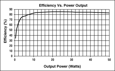
Figure 10 shows the output-voltage regulation of the power supply from 0A to 10A of output current. Voltage measurement was done at output-voltage sense points.
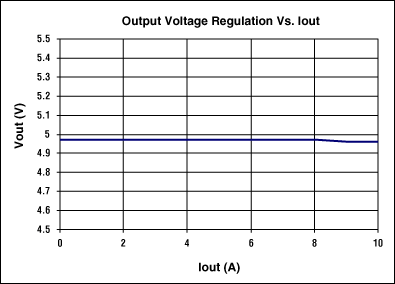
Table 3. Power-Supply-Performance Data
| Pout | 50W |
| Vin | +36V to +72V or |
| Vin | -36V to -72V |
| Vout | +5V |
| Iout | 10A |
| Initial Output-Voltage Set-Point Accuracy | ±3%* |
| Output-Voltage Regulation Measured | 0.3%, over line and load |
| Efficiency Measured | 85% @ 48V and 25W |
| Input-Output Isolation | 1500V for 1sec |
| Switching Topology | Feed-forward compensated |
| Forward Dimensions | 4.05″ x 1.3″ |
*Initial set-point accuracy can be improved with external component trimming or by using a better-tolerance output-voltage sense-resistor divider.
PCB Layout and Component Placement
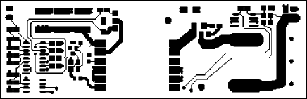
As with any other switching power supply, component placement is very important. Because of the primary to secondary isolation, the primary and secondary grounds are separated. Figure 13 shows the separation on both sides of the PCB. The layout of the board can be changed to accommodate different footprints. In addition, the power FET and output rectifier should be mounted on a heatsink for best thermal management. In this implementation, both of these components were mounted on the noncomponent side of the board with their tabs exposed so that they could easily be mounted on a heatsink.
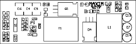

The critical layout points are as follows:
- The distance from the secondary transformer leads to diode D4 should be kept to a minimum. This will improve EMI as well as the effective available power transfer.
- The bypass capacitors C4/C5/C6 should be as close as possible to lead 1 of T1. Lead 2 of T2 should be as short as possible.
- The current-sense resistor R6 should be as close as possible to the source of Q1 and should return with a very short trace either to ground plane or to the negative lead of bypass capacitors C4/C5/C6.
- The gate drive loop of Q1 also must be routed over ground plane or be very short.
- All other components must be placed close to the control IC.
- Relevant trace spacing (relating to trace creepage) must be observed.
Conclusion
Here, we have described the design of a 50W, telecom power supply that uses a new control IC developed specifically for this purpose. The design offers a lower-cost alternative to ready-made bricks, while providing respectable electrical performance. The circuit can be built in a relatively small area and optimized to fit a custom footprint.


 combined with superior switching performance")


