


Abstract
This article presents rigid-flex circuit board design guidelines for the development of a core body temperature (CBT) sensor device. These guidelines are generic in such a way that they can be applied to multiple temperature sensing applications requiring high accuracy (± 0.1°C).
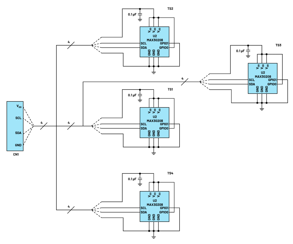
The recommendations herein were implemented in the joint development of a CBT sensor device by Texas A&M and Analog Devices, Inc. (ADI). The CBT device employed four MAX30208 temperature sensor devices in an assembly that measured heat flux for estimating a subject’s CBT accurately.1,2
Introduction
The guidelines offered are intended to aid a designer in identifying and mitigating multiple areas of potential concern while designing high accuracy (±0.1°C) temperature sensing circuits. This is demonstrated via an example of a recent CBT design where thermal, electrical, and mechanical aspects were concurrently addressed with appropriate trade-offs implemented. These design considerations shall assist the designer to:
- Learn how to recognize the design challenges, trade-offs, and mitigation techniques associated with the development of an accurate CBT sensing device.
- Learn how to design a reliable rigid-flex printed circuit board for remote patient monitoring applications.
- Apply design guidelines for heat flow and mechanical structure considerations.
- Apply design guidelines for rigid-flex PCB manufacturing.
Overview of the CBT Device Design
The CBT patch was developed as a flexible wearable thermal sensing device that accurately estimates human CBT (Figure 1a). Figure 1b highlights the main components of the thermal device. The device comprises four temperature sensors (MAX30208) separated by the materials with different thermal conductivities to accurately quantify CBT. The temperature sensors provide 0.1°C accuracy with a supply voltage of 1.8 V, supporting low power operation. One temperature sensor device is located at the center of the PCB, two temperature sensor devices are located at the PCB middle and edge, and the fourth sensor is located on the tip of a flexible finger, which is bent back in the neck area towards the center of the rigid-flex PCB (Figure 1c).
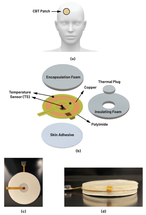
The CBT patch is intended to monitor human patients in pre-op, operative, and post-op surgery settings. Such environments have typical ambient temperature ranges of 20°C to 24°C and maximum air convections rates of 5 W/m2 K. Normal forehead core body temperatures are in the range of 36°C to 38°C. Below 36°C is a condition called hypothermia and above 38°C is a condition called hyperthermia. Both conditions are considered serious and subsequently necessitate monitoring during all phases of surgery.
Layout Design Considerations for Heat Flow
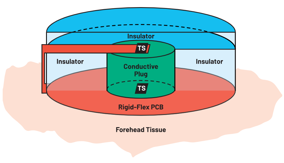
The CBT patch device is designed to measure vertical heat flow from the human tissue surface using two MAX30208 temperature sensing devices. This is shown in Figure 2. The MAX30208 temperature sensors are shown with TS labels. The other two temperature sensors (shown in Figure 1) help account for lateral heat losses. Data from the temperature sensors, combined with thermal models for the conductive plug and insulator, are used to accurately estimate CBT on human foreheads.
To accomplish this task, the rigid-flex PCB with temperature sensing circuits needs to:
- Incorporate temperature sensors with high accuracy.
- Have low enough power consumption (temperature sensor) to not adversely impact the thermal system of interest.
- Have signal traces that are adequate in size for electrical signal transmission.
- Have signal traces with dimensions that minimize heat flow from (or to) the MAX30208 temperature sensor such that the thermal system is not adversely impacted.
- Have signal traces with dimensions that minimize heat radiation from the PCB traces (that is, I2R loss) into the conductive plug area.
By implementing select thermally conductive/insulating materials, the physical structure establishes a design allowing for an accurate estimate of CBT on the forehead. Combining this mechanical design with accurate low power temperature sensors, such as the MAX30208 device, a successful design is produced. However, the electrical connections necessary for electronic devices conduct heat as well—a phenomenon not desired!
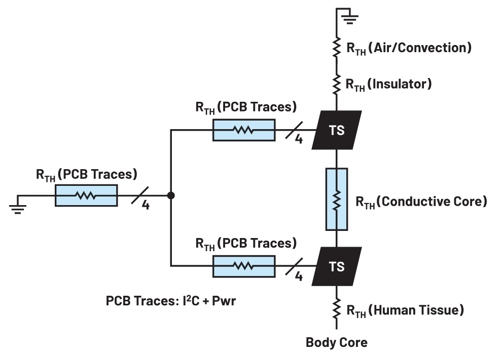
Figure 3 highlights the main heat flow paths of interest. One would like to design the thermal resistance of the PCB traces to be very large compared to the conductive plug to keep these heat loss (or gain) errors negligible.
As heat and electricity are both transported via electron motion, they are intimately related to each other. According to the Wiedermann-Franz Law3, the ratio of thermal to electrical conductivity is approximately constant for different metals at the same temperature. In other words, what’s good for thermal resistance is bad for electrical conduction, and vice versa. Fortunately for this use case, with a fairly limited temperature range, the application of alternate metals from those commercially available was not required.
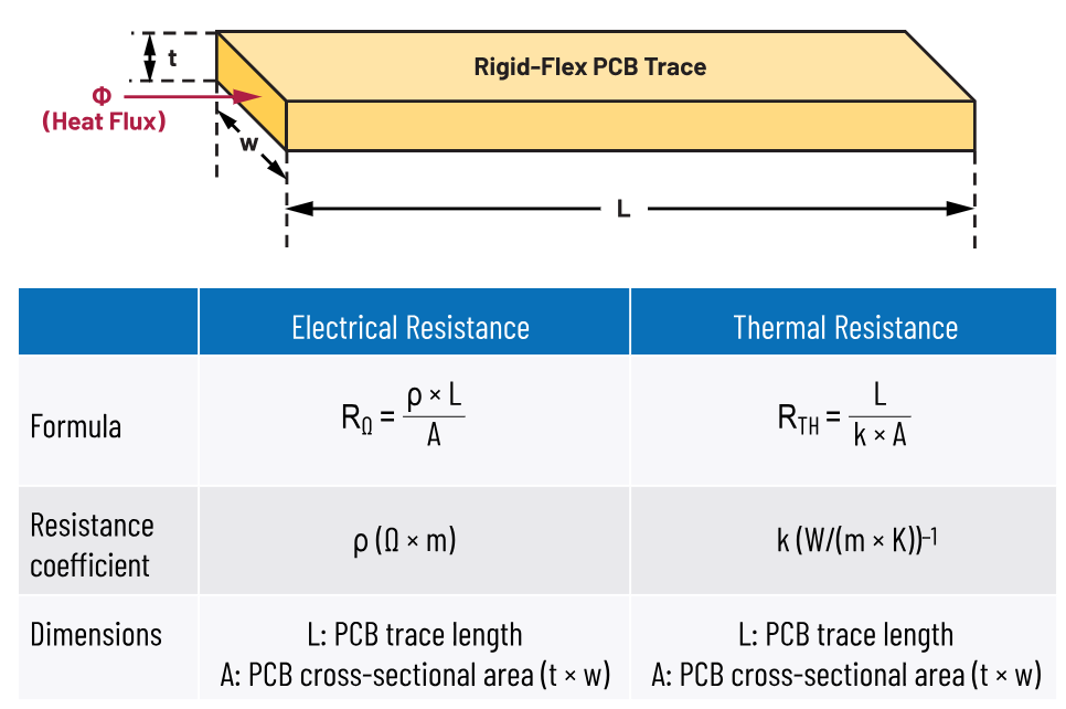
While implementing a commercially available metal for signal and power traces, a thermal-electrical design trade-off is still needed for the rigid-flex interconnections. The design formula for electrical and thermal resistance is given in Figure 4. The thinner and longer the rigid-flex PCB trace is, the larger the thermal resistance. This provides a means to set the thermal resistance greater than the primary conductive plug, minimizing thermal leakage (that is, error) from the CBT thermal system. Unfortunately, the electrical resistance increases as well. This can lead to several adverse effects such as power line voltage drop, increased temperature of the PCB trace, and an increased RC time constant for the I2C communication lines.
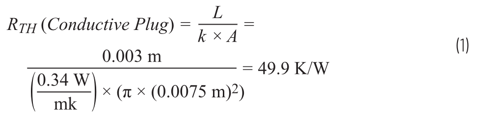
Before considering the PCB traces, the conductive plug thermal behavior should be first evaluated to establish a design baseline. The heat path has a cylindrical form factor as shown in Figure 5.
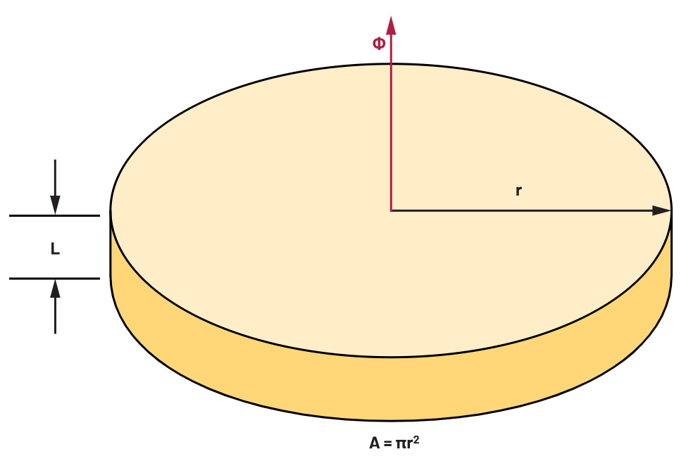
The thermal resistance of the CBT patch conductive plug can be calculated knowing the material conductivity and dimensions as follows:
Turning our attention to the thermal resistance of the PCB trace, we need to consider several issues:
- The PCB trace thermal resistance should be significantly greater than the CBT patch conductive plug (for example, RTH (PCB trace) ≥ 100• RTH (conductive plug)).
- Power requirements of the temperature sensing device (for example, the MAX30208) need to be known and the PCB traces dimensions designed to minimize associated heat loss from the traces into the BCT patch conductive plug. This is greatly mitigated by employing a low power temperature sensor device such as the MAX30208.
- The PCB traces that are in contact with the conductive core need to be checked for potential heat radiation. The smaller the traces for thermal consideration, the larger the I2R heat transfer error can occur.
- The total length of the PCB traces for a given cross-sectional area should be adequate to ensure a large thermal resistance (compared to the CBT thermal conductive plug).
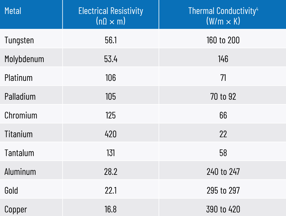
Figure 6 displays the thermal/electrical characteristics of various utilized PCB metals. As the commonly implemented metals in PCB manufacturing (for example, gold, copper, silver, and aluminum) have thermal and electrical conductivities within the same order of magnitude, the specific material selection does not dominate our choice. Copper was chosen for cost, availability, and mechanical flexibility (to be discussed in the next section).
While copper’s thermal conductivity is over 1000 times larger than that of CBT patch conductive plug, the dimensions of the thin copper traces were chosen to achieve a much greater thermal resistance than 49.8 K/W (that is, the CBT patch conductive plug thermal resistance).
The PCB traces are composed of ½ oz copper (17.3 µm thick) core, 1.5 µm nickel layer, and a 0.1 µm gold outer layer. Given the relative dimensions of the these, all forthcoming calculations assume only the copper core PCB traces.
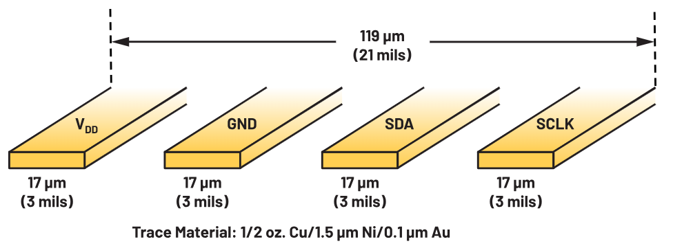
Each PCB trace was fabricated with 76.2 µm (3 mil) widths, yielding:
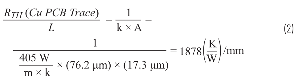
Note: While a smaller trace width is desired for increased thermal resistance, PCB fab houses will have constraints on their minimum trace widths. For example, we initially wanted 2.5 mil trace widths, but eventually went with the fab house recommendation of 3 mil trace width for our prototype build.
Further, each MAX30208 temperature device has a set of four (4) traces of equivalent dimensional design. See Figure 7. Thus, the overall thermal resistance is decreased by four times (that is, four thermal paths in parallel), yielding:
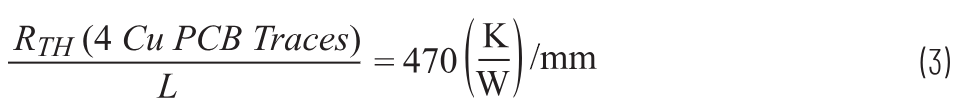
Figure 8 highlights the approximate thermal resistance of each set of four temperature sensor I/O lines to the output connector, CN1.
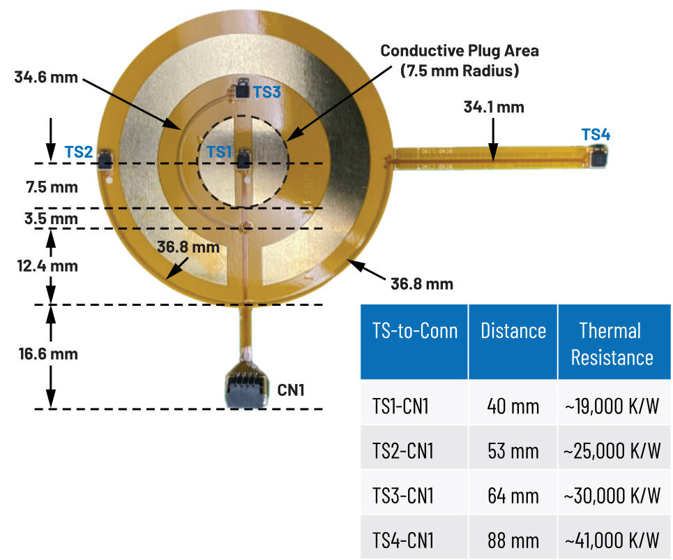
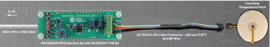
The set of four I/O signal lines with the lowest thermal resistance (for example, TS1-CN1) is about 380× larger than the CBT conductive plug. This meets our design target of being greater than or equal to 100× larger! Additionally, this is further improved by the bus wire extension from the connector CN1 to the MAX30208EVSYS interface board. Our prototype system used 200 mm (7.9 inches) long, 28 AWG wire that is wrapped around the top of the ear down to the interface board.
Note: While the thermal resistance is adequate to isolate the heat conduction inside the conductive core, the heat generated in the interface board needs to be considered. If large enough, heat energy can be conducted back into the CBT patch causing error. This was not an issue for our evaluation system.
Thermal Error Mitigation of the Electrical System
Turning our attention to the electrical system, we shall look at two main areas of concern: (1) the heat generated from the MAX30208 device (for example, self-heating), and (2) the heat generated from the PCB trace(s) (for example, heat radiation). Both sources can adversely affect the performance of the thermal system by sourcing (or sinking) heat energy into (or out of) the CBT patch. Figure 10 shows a representative schematic for the MAX30208 circuit design.
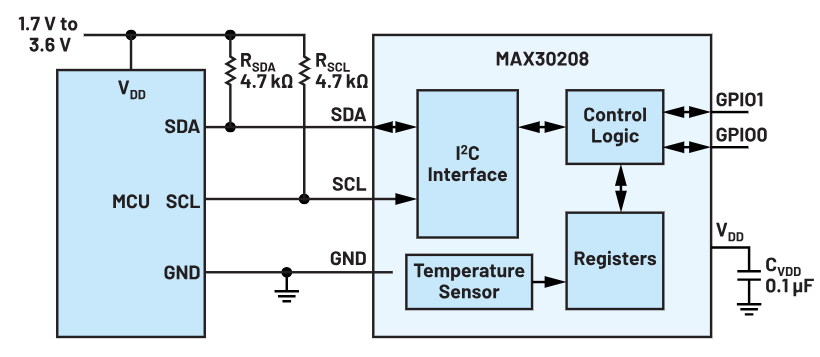
The MAX30208 (±0.1°C accurate, I2C) digital temperature sensor was selected for its accuracy and low power requirements. The CBT patch electrical system was powered with a regulated 1.8 VDC power supply located on the MCU interface board. The I2C pullup resistors, being a significant source of heat energy, are located on the MCU board. There are no I2C pullup resistors implemented on the CBT patch rigid-flex PCB.
Table 1 lists the current and voltages levels on each I/O pin for operation at 37°C. These values were extrapolated from the MAX30208 data sheet electrical table and associated TOC figures.
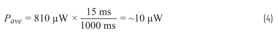
Most of the power dissipation comes from the I2C signal lines and the power supply line yielding approximately 810 µW of power if operated continuously. As the temperature signal does not change very quickly, periodic sampling can be employed. Not only does this aid in data management but allows us to reduce the overall power requirements. This in turn will help mitigate heat dissipation of the MAX30208 device and associated signal and power traces.
The MAX30208 implements a typical 15 ms integration period. With a sampling rate of 1 Hz, the average power consumption is approximately:
While package thermal resistances are typically reported in data sheets, a designer needs to be cautious in their use for heat flow estimates. Both θjA (thermal resistance, junction-to-ambient) and θjC (thermal resistance, junction-to-case) are evaluated per JEDEC environments, which can be quite different than the actual application. They are commonly used as figure-of-merit values for comparing competing devices against each other.
As such, it is not recommended to use the ambient temperature to predict the junction temperature.5 Especially since the temperature sensors in this application are sandwiched between insulating and noninsulating materials.
As the MAX30208 temperature measuring circuit is on the integrated circuit, the associated self-heating of the die is what we are most interested in. This device was designed to measure the external temperature on the top (or bottom) of the package. Assuming that the case temperature is at the same die temperature, we can estimate the temperature error due to self-heating as follows6:
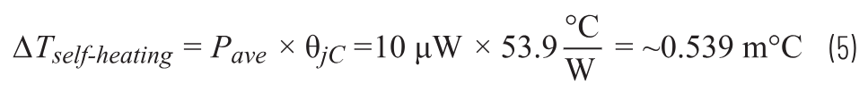
Given that we are over 100 times smaller than the accuracy of the MAX30208 (for example, ± 0.1°C), the assumption that the case and die are at same temperature is acceptable.
Note: This may not always be the case wherein the die temperature requires characterization. One useful technique is to use an ESD diode, commonly implemented on IC I/O lines, as a temperature sensor to characterize the temp rise of the IC die.
Next, we turn our attention to the I2R heat radiation of the PCB traces in the conductive core area. Referring to Figure 8, the distance from TS1 or TS4 to the outer edge of the conductive core is 7.5 mm. Using the formula for electrical resistance (see Figure 4) of a single PCB trace and the resistivity of copper, we calculate the following:
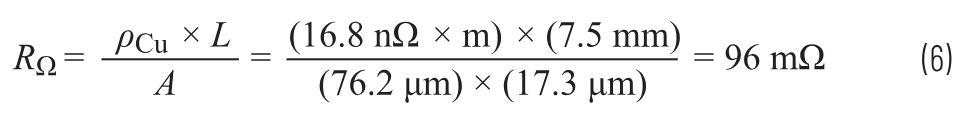
Using the maximum current of 383 µApk for the SCL and SDA signal lines, we calculate the heat radiation value for a single PCB trace as follows:

This is negligible to the thermal system of interest. Further, this is an absolute worse-case level if periodic sampling is not implemented. In conclusion, the thermal errors originating from both the MAX30208 self-heating and PCB trace heat radiation in the conductive core have insignificant effects.
The line voltage drops are within acceptable levels as well. The longest wire length is 88 mm (TS4 to CN1) plus 200 mm of 28 AWG (0.32 mm diameter) wire, which connects to the MAX3020x interface board. Using the same formula for electrical resistance for the longest line, we calculate the following:
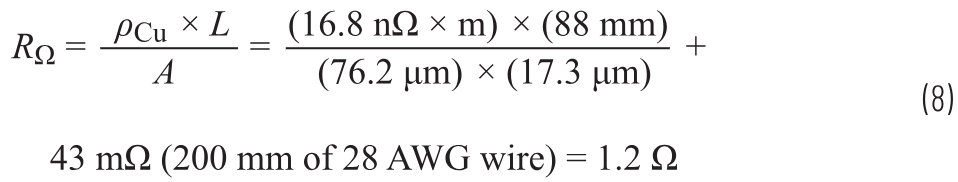
Using the maximum current of 67 µA for VDD, we calculate the line voltage drop as follows:

This is small enough that no issues with respect to power supply rejection will arise.
While we have highlighted major thermal and electrical design considerations for the rigid-flex PCB used in the CBT patch, finite element analysis (FEA) is highly recommended. An FEA (thermal) was conducted for transient analysis validation before prototyping the first patches. Thermal and electrical capacitances have not been discussed in this article. While neither had any significant effect on performance in this application, it is recommended that these be analyzed during the design phase as well.
Figure 11 shows a schematic diagram of the CBT device that highlights the PCB trace branches used to mitigate heat flow as well as implement electrical interconnections in the 2-layer polyimide rigid-flex board.
Layout Design Considerations for Mechanical Construction and Reliability
The rigid-flex circuit is a hybrid construction of a conventional rigid PCB and a flexible circuit. While this circuit is designed to have mechanical compliance for conformal attachment to a human forehead, there are several critical locations requiring rigidity. These are:
- The nine SMT component attachment sites.
- The circuit finger extending from the circular circuit area to the temperature sensor (TS4).
- The circuit finger extending from the circular circuit area to the connector (CN1).
- The rigid-to-flex circuit boundaries.
SMT components are typically attached using solder reflow. As such, the assembled components may need to be located on rigid PCB material to maintain solder joint integrity. SMT components soldered onto flex PCB material must be handled with care due to reduced strain relief. Even if the use case involves relative freedom from physical disturbance, handling and next-level assembly needs to be considered for long term reliability.
Typical PCB stiffeners are implemented using FR4, polyamide, polyimide, and/or metal. In our CBT patch, we use a 4 mil thick polyimide for the flexible areas with a 12 mil thick polyimide for the stiffened areas. For stiffening purposes, the flexible finger circuits were reinforced with metal segments.
The CBT patch prototype is manufactured as a flat rigid-flex assembly subsequently requiring two static bends. Shown in Figure 10, the circuit finger extending from the circular circuit area to the TS4 temperature sensor needs two 90° bends for the final assembly.
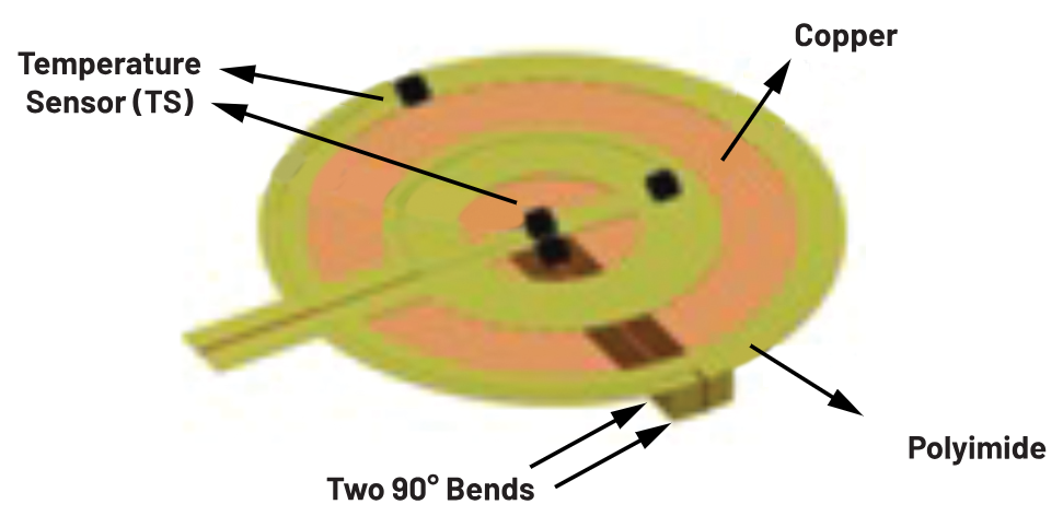
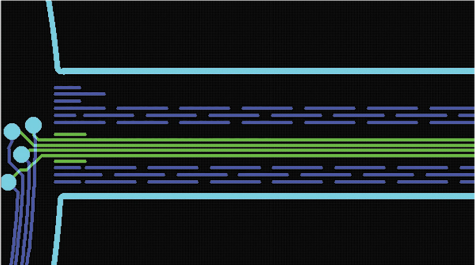
Brick-pattern metal segments are used to construct the TS4 flex finger design such that the fatigue imposed by the one-time static bends are mitigated. Figure 13 shows the staggered brick-pattern stiffeners as well as the neck-area reinforcement to mitigate mechanical stresses to the rigid-to-flex boundary. Furthermore, the breaks in the brick pattern eliminate thermal conductivity along these metal paths. This design technique is also mimicked on the circuit finger extending from the circular circuit area to the connector (CN1).
Other areas of consideration include avoiding 90° corners (for example, points of stress concentration) and the potential implementation of preform fabrication.
Manufacturing Considerations and Guidelines
To produce a robust and reliable design, it is recommended that a designer work closely with the PCB fab and assembly house(s). Design details of all electrical, thermal, and mechanical aspects should be reviewed prior to first article fabrication. In many instances, the fab/assembly house(s) has alternate materials and/or techniques that can be implemented for design enhancement.
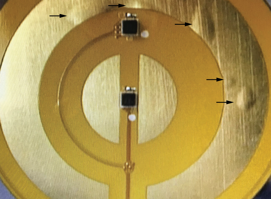
During the development of the CBT patch rigid-flex PCB assembly process, several significant hurdles had to be overcome: The solder reflow material used, and the solder reflow profile. Originally, standard reflow solder was used resulting in delamination (see Figure 14). This is particularly unfavorable given the fact that air-pockets, acting as insulators, will influence the heat flow through the rigid-flex PCB. This was eventually mitigated by using an alternate low temperature eutectic solder. The solder reflow profile had to be fine-tuned over several batches to achieve an acceptable yield.
Conclusion
This concludes the article in which design considerations are discussed to help mitigate technical impediments for high accuracy heat flow applications. Specifically, how the implementation of an accurate, low power device (for example, the MAX30208 temperature sensor) can fulfill the performance requirements for a core body temperature patch. With suitable component selection and application of good design techniques that properly balance thermal-electrical-mechanical trade-offs, one can achieve a successful design.


 combined with superior switching performance")


