

Abstract
This article discusses the challenges in developing state-of-the-art ultrasound machines. An existing evaluation platform can be used to reduce both system development costs and the characterization time of the transmit block of an ultrasound system. Step-by-step procedures are presented in this article on how multiple channels may be synchronized, a crucial concept in beam steering and one that is unique to medical imaging.
Introduction
In any new technology development process, before commercializing new models or next-generation ultrasound machines, manufacturers undergo stages of hardware development and testing, and system integration and validation. Developing a high channel count imaging ultrasound subsystem is expected to take many years of effort. Furthermore, jumping into hardware prototyping of the beam steering or transmit subsystem with limited knowledge of system considerations can be costly as it can result in multiple revisions of the hardware prototype. Now, a complete system (prototype board and open-source software) can be used to emulate the operation of an ultrasound machine subsystem, thereby reducing development cost and time-to-market for ultrasound manufacturers.

Arduino-Based TxDAC Evaluation Board with Open-Source Mbed Software
The AD9106-ARDZ-EBZ evaluation platform is compatible with Arm-based Mbed-enabled boards like SDP-K1 and is designed to connect to Arduino Uno headers. The evaluation setup can be powered by USB only and does not require a high frequency waveform generator for clock input. The evaluation board by default uses an on-board 156.25 MHz crystal oscillator as a clock source but provides an external clocking option. DAC outputs can be transformer-coupled or evaluated with on-board amplifiers, the only time a 7 VDC to 12 VDC 30 W AC-to-DC adapter is needed. See Figure 1.
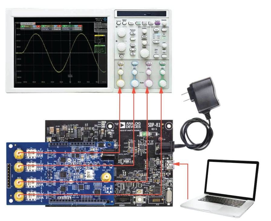
Along with the hardware, example open-source codes are provided on the evaluation board web page and can be used as starting point for developing firmware for targeted applications. The evaluation boards and the example source codes can be customized to work with other Mbed platforms. The new evaluation system eases prototyping because it can be easily integrated into existing systems.
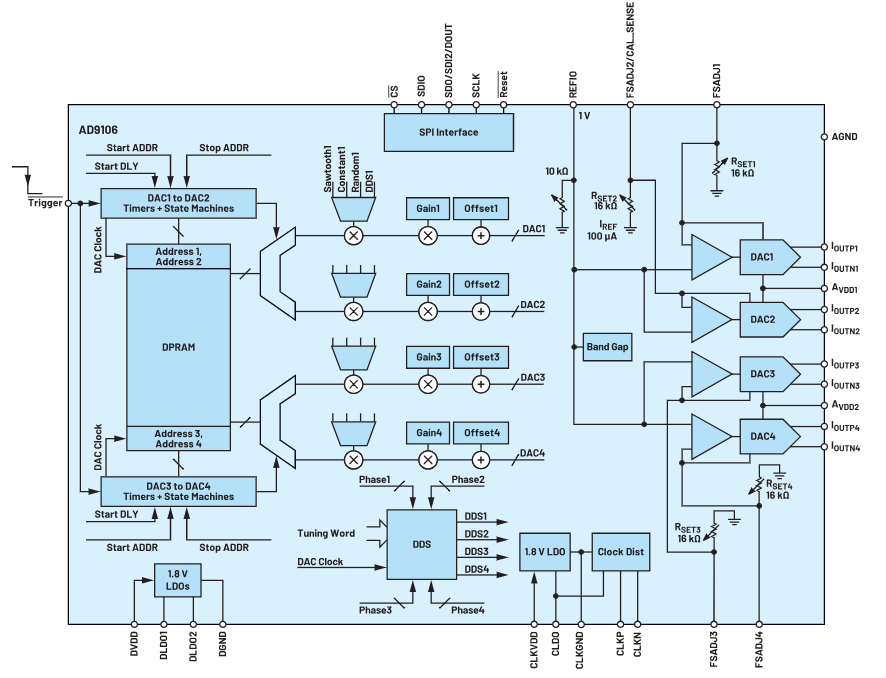
The evaluation board is populated with the AD9106 quad, low power, 12-bit, 180 MSPS, TxDAC, and waveform generator. The DAC’s high sampling rate is ideal for ultrasound operating frequencies that are in the 1 MHz to 40 MHz range, with external imaging machines typically using frequencies of 1 MHz to 15 MHz, while intravenous cardiovascular machines use as high as 40 MHz. Moreover, the AD9106 is highly integrated and has an on-chip pattern memory for complex waveform generation and a direct digital synthesizer (DDS) with a 24-bit tuning word allowing 10.8 Hz/LSB frequency resolution. It is also highly programmable because pattern period, start delays, gain, and offset can be independently varied for each of the four DAC channels. In addition, it is low power (dissipating 78.8 mW/channel, 315.25 mW total, at 3.3 V, 4 mA output, and 180 MSPS), which is an important consideration for large multichannel systems like an ultrasound machine.
Improving Accuracy and Image Resolution of Ultrasound Devices
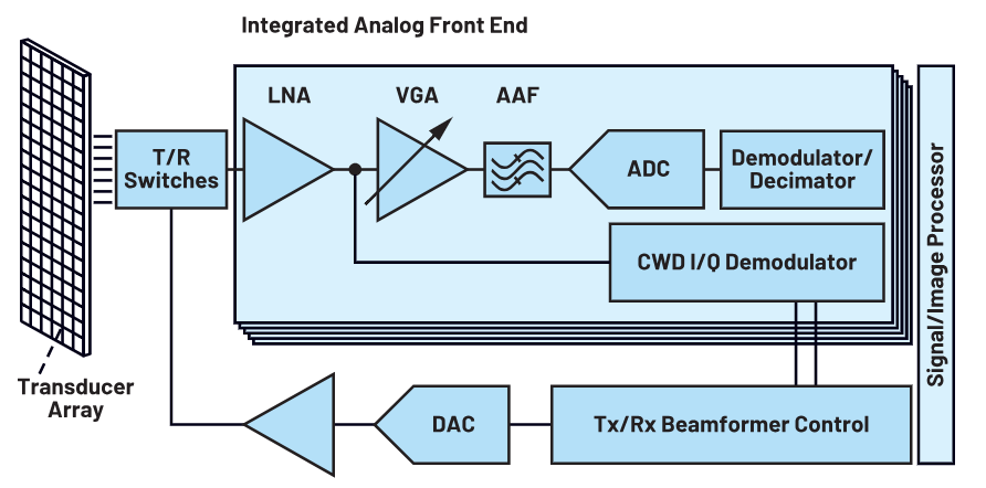
Cart-based ultrasound systems are superior to handheld devices in terms of image quality or resolution mainly because of the big difference in the number of channels. Channel count, however, may vary from manufacturer to manufacturer. Since cost and power consumption are significant considerations in a large system such as the ultrasound machine, some techniques are used to minimize both factors. In a typical ultrasound signal chain in Figure 3, determining the number of channels is straightforward if we consider that there is one receiver path (integrated analog front end) for every transmitter path (DAC + high voltage amplifier), which drives one element in the array of transducers at the probe tip. With this assumption, we can say that number of channels in an ultrasound system can range from 16 to 256. The number of channels in high end systems, most of which are cart-based, is 64 or greater. A range of 16 to 64 channels is more common for portable, mid to low end systems.
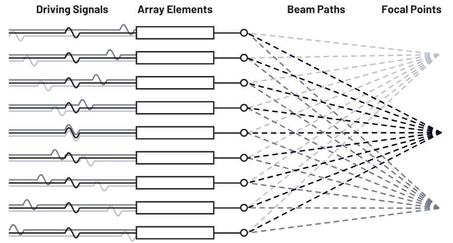
In the transmitter path of an ultrasound system, a beam of acoustic energy or sound waves is swept around the body. The sound waves are converted from electrical signals by the piezoelectric transducer elements at the probe tip. As shown in Figure 4, the phase and amplitude of each of the electrical or transmitter signals are programmed such that the incident beam of energy is directed along a line into the body. The sound waves bouncing off organ tissues are converted again to electrical energy by the transducer elements. The location or distance of the target will be represented on the screen based on the time delays from element to element in the transducer array. Thus, the synchronization or being able to control the delay between transmitter signals is crucial in displaying an accurate image of the inside of the human body.
Requirements for Multichip Synchronization
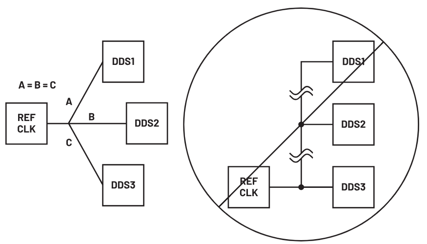
For successful synchronization of multiple DDS DACs like the AD9106, there must be control over the differential clock input (CLKP and CLKN) and the falling edge of the TRIGGER pin.
To achieve the first requirement for synchronization, careful clock distribution practice in the layout of the PCB should be employed. Refer to Figure 5. This will minimize phase differences between REF CLK edges that result in proportional phase differences at the DDS outputs.
Since pattern generation is signaled by a falling edge at the TRIGGER pin of the AD9106, the next requirement for synchronization is to ensure coincident TRIGGER edges. The layout technique in Figure 5 can also be applied to the TRIGGER PCB traces routed from the digital outputs of a controller to each individual AD9106 device.
Using the AD9106-ARDZ-EBZ to Evaluate Multichip Synchronization
To evaluate the synchronization of multiple AD9106 DACs, two AD9106 evaluation boards and an SDP-K1 controller board can be used.
Materials
- Two AD9106-ARDZ-EBZ boards
- USB cable for board-to-PC connection
- SDP-K1
- One 12 V wall wart
- Signal generator
- Variable length SMA-terminated cables
- One SMA-terminated T-splitter
- Female to female Arduino connector wires
Hardware Setup
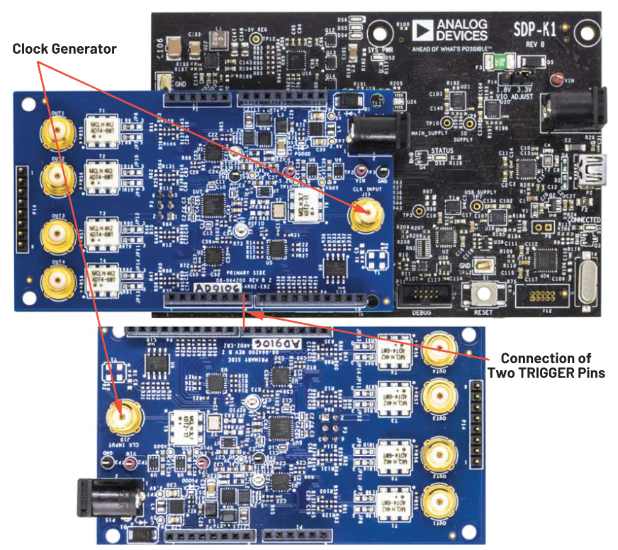
Before connecting the three boards, configure the two AD9106-ARDZ-EBZ boards such that DAC outputs are connected to the on-board amplifier and the DAC clock is supplied by an external source connected to J10. Refer to Figure 14b in the Eval-AD9106 Wiki User Guide for the proper JP1 and JP2 connections. Also, set up one of the AD9106-ARDZ-EBZ boards such that the CSB pin of the device on board is connected to the alternate GPIO pin (R39 is installed instead of R38). Ensure that the VIO_ADJUST of SDP-K1 is set to 3.3 V.
Next, the connections to the clock inputs and TRIGGER pins of each board shown in Figure 7 should be set up before the rest of the connections in Table 1. Attach Board 1 to the SDP-K1 Arduino Uno ports then place Board 2 at 180° with respect to Board 1 so that the TRIGGER pins of both boards are side to side. This is the shortest connection of TRIG2 to SDP-K1 digital out resulting in TRIG1 and TRIG2 paths being approximately equal.
Then, connect the output of a high frequency waveform generator to a split SMA-terminated T-splitter to which varying lengths of SMA-terminated coaxial cables can be hooked up.
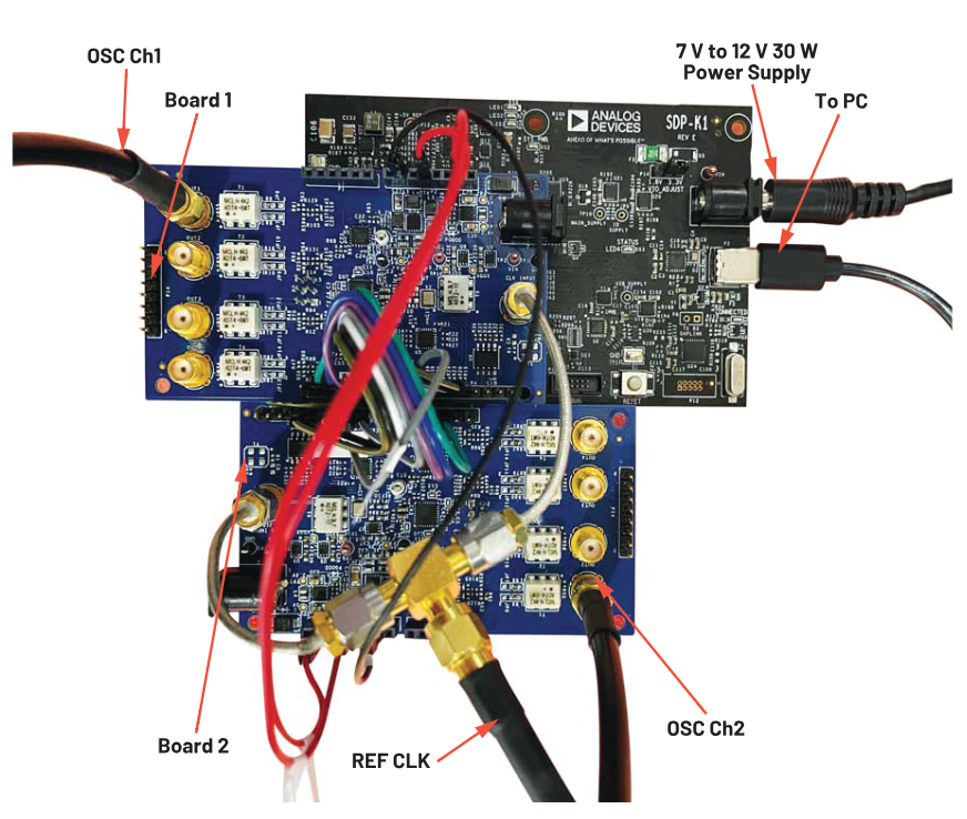
The actual setup with all connections applied is shown in Figure 8. Board-to-board connections are summarized in Table 1.
| SDP-K1 Arduino Uno Connectors | Connected Nets on AD9106-ARDZ-EBZ | ||
| Pin No. | Pin Functions | Board 1 | Board 2 |
| P2.1 | NC | ||
| P2.2 | IO_PWR_SUPPLY | IOREF | IOREF |
| P2.3 | MAIN_RESET | RESET | RESET |
| P2.4 | SDRAM_&_ARDUINO_PWR_SUPPLY (3.3 V) | 3.3 V | 3.3 V |
| P2.5 | +5V_CON | 5 V | 5 V |
| P2.6 | GND | GND | GND |
| P2.7 | GND | GND | GND |
| P5.1 | ARDUINO_GPIOO/RX | VIN | VIN |
| P5.2 | TX + 1 | ||
| P5.3 | GPIO2 | EN_CVDDX | EN_CVDDX |
| P5.4 | GPIO3/PWM | ||
| P5.5 | GPIO4 | SHDN_N_LT3472 | SHDN_N_LT3472 |
| P5.6 | GPIOS/PWM | ||
| P5.7 | GPIO6/PWM | ||
| P5.8 | GPIO7 | TRIGGERB | TRIGGERB |
| P4.1 | GPIO8 | RESETB | RESETB |
| P4.2 | GPIO9/PWM | SPI_CSB_ALT | |
| P4.3 | GP1010/PWM/CS | SPI_CSB_DFLT | |
| P4.4 | GPIO11/PWM/MOSI | STD_SPI_MOSI | STD_SPI_MOSI |
| P4.5 | GPIO12/MISO | STD_SPI_MISO | STD_SPI_MISO |
| P4.6 | GPIO13/SCK | STD_SPI_SCK | STD_SPI_SCK |
| P4.7 | GND | GND | GND |
| P4.8 | AREF | ||
| P4.9 | SDA | ||
| P4.10 | SCL | ||
Software
An example source code developed on Mbed open-source software is available. Minimal changes can be made to these source codes described in detail in the wiki page to independently program each device in the two evaluation boards via SPI. Register values, specifically for Example 3 (DDS-generated sine waves with different start delays and digital gain settings), and other parts of the code can be easily customized. After modifying the code, compile the program using the Mbed online compiler. Then drag and drop the generated binary file to the SDP-K1 drive. The same process can be done for other applications.
Directions
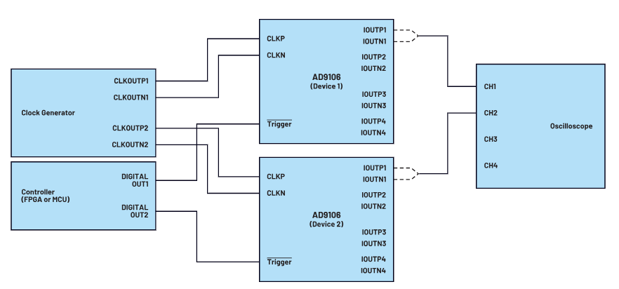
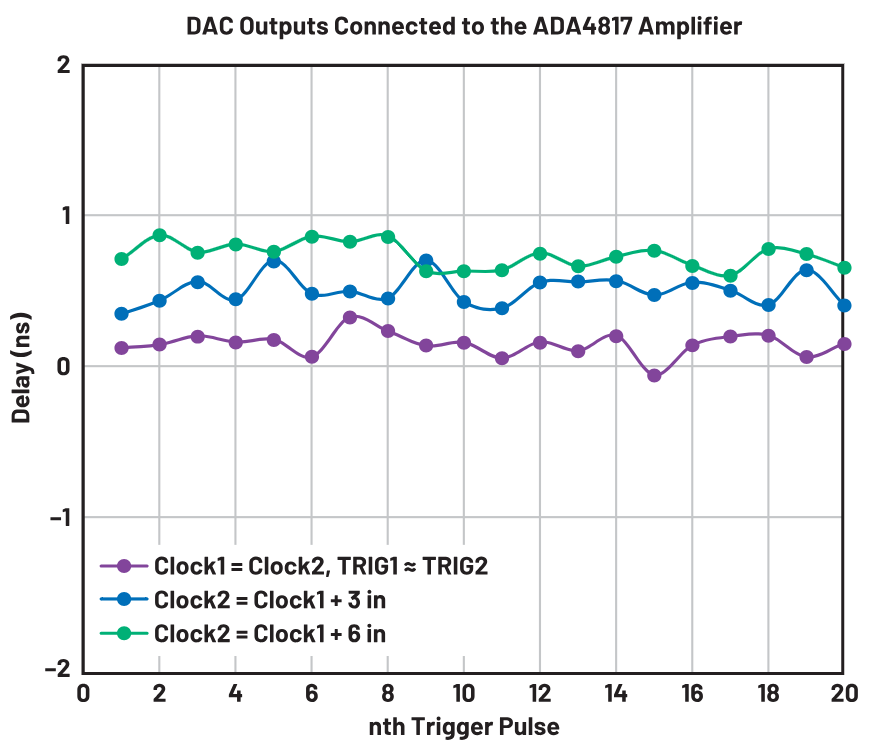
As shown in the simplified diagram in Figure 6, device-to-device output synchronization is performed by measuring the delay between the same DAC output channel, that is, Channel 1 of multiple devices. The effect on synchronization of varying the TRIG2 (controller board to Board 2) with respect to TRIG1 (controller board to Board 1) and varying the length of connectors for Clock 2 (clock generator to Board 2) with respect to Clock 1 (clock generator to Board 1) can be observed using an oscilloscope.
Results
Figure 9 documents the measurement when varying the trigger connector lengths while Figure 10 documents the measurement when varying the clock connector lengths.
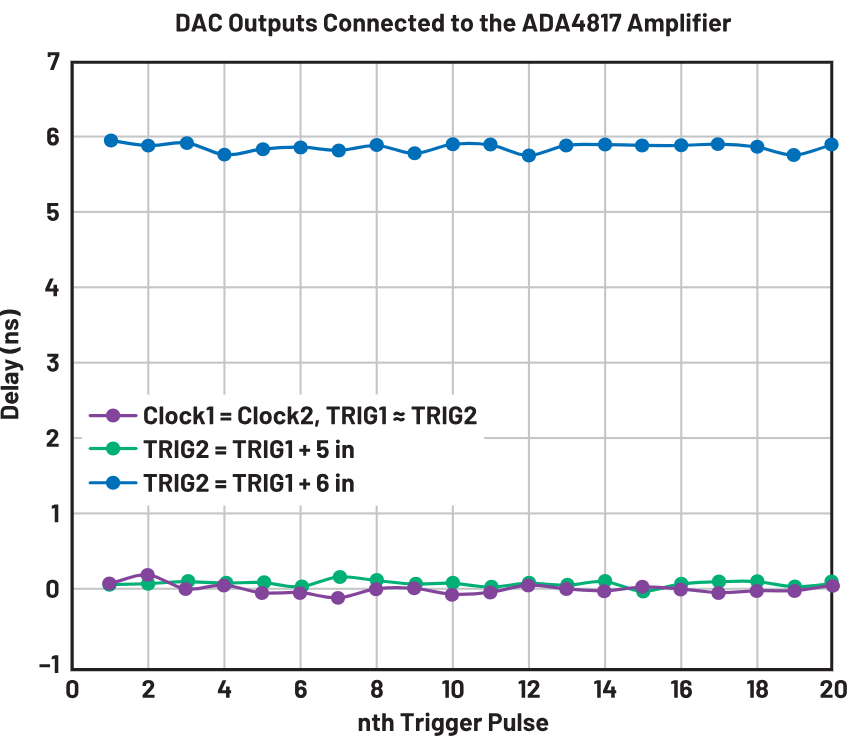
If TRIGGER pins are connected to digital outputs with drive characteristics like that of STM32F469NI, the microcontroller on SDP-K1, TRIGGER trace tolerance can be up to 5 inches to maintain device-to-device synchronization.
Matched clock input traces will result in the shortest device-to-device output delay but depending on tolerable delay in a specific system, clock trace length tolerance can be adjusted accordingly.
Conclusion
In ultrasound manufacturing, shortening the development process and time-to-market can be achieved by taking advantage of the design flexibility and customization offered by the AD9106 evaluation platform. There is no need to design a new transmit subsystem prototype to be able to evaluate the synchronization of multiple transmit DACs, like the AD9106. Instead, this can be done by using two AD9106-ARDZ-EBZ boards, one SDP-K1 controller board, and making minimal adjustments to the example Mbed codes.


 combined with superior switching performance")


