


Abstract
With the introduction of the AISG v3.0 standard in 2019, many use cases were implemented for antenna line communication. While these changes had little to no impact on the physical layer of operation, one systematic change was obvious: every RF connection on the cellular tower would now require AISG communication to service the ping function. This article summarizes changes on the hardware level and demonstrates how features of an AISG modem with a 4:1 multiplexer can help system designers implement the standards requirements with fewer components and less development overhead.
Introduction
The proliferation of cellular networks and handsets over the past decade has resulted in an exponential need for electronics to support the mobile communications infrastructure. A simultaneous demand for more bandwidth is also pushing network providers to continuously expand their coverage while increasing cell density; in turn, this has boosted the need for infrastructure hardware.
Over 15 years ago, manufacturers began to standardize the interoperability of cellular radio equipment, allowing more variation in assembling cellular base stations with antenna gear, amplifiers, etc. This communication standard was first established by the Antenna Interface Standards Group (AISG) in 2003 and 2004. The AISG standard continues to evolve with market expansion. Several features are considered to meet the interoperable communications needs of today and the future.
AISG v2.0 and the Physical Layer Modem
Integrated modulator-demodulators (modems) were introduced in 2009 to provide a complete, focused solution for translating between the ubiquitous RS-485 interface and a 2.176 MHz OOK signal, defined by the communication standard riding on the same cable as the cellular RF band. The IC solution allowed for a much more compact system design, saving space, power, and hardware. In addition, the integrated modem provided the reliability of a simple, proven, factory-tested device in one small package.
AISG v3.0 Standard
An upgrade to the successful standard was put forth by the AISG in 2019. This evolutionary step was built upon the success of previous generations with the intent to add new features, while maintaining the core interoperability of primaries and their managed antenna line devices (ALDs).
The AISG v3.0 feature set includes device discovery, connection mapping, and multiprimary control. While a system designer can find the standard to be a helpful upgrade for many higher level functions, the physical (PHY) layer remains unchanged from v2.0 to v3.0. Consequently, all modems originally introduced with v2.0 are still fully compatible with the AISG v3.0 standard.
Need for More than One AISG Channel
Although the step from AISG v2.0 to v3.0 had very little impact on the physical layer of the system, the v3.0 standard requires the ability to initiate and detect a ping packet on all the connected RF channels. This requirement facilitates the mapping of cable connections, allows the end user to identify multiple primaries and secondaries, and provides a tool for fault detection during initial assembly and maintenance. Although the need for each channel to have awareness of AISG helps the end user, it places a large burden on the hardware designer to include communication capabilities on all possible RF channels, where previously it was only necessary for one.
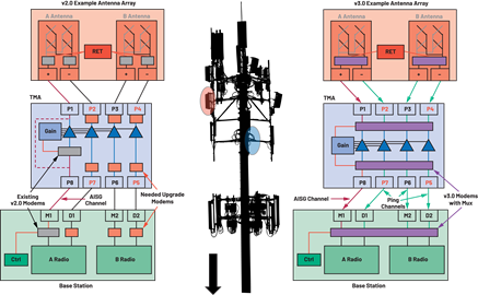
Trying to convert an AISG v2.0 architecture directly into a v3.0 compatible application could require over twice as many modems as previous generation designs—going from six modems (gray blocks in Figure 1) to 15 (gray plus red blocks).
In Figure 1, two modems remain for each antenna pair to maintain compatibility across base station providers. However, seven or eight modems are required on the tower mounted amplifier (TMA): four listening on the ports running to the antenna array (upstream) and four used on the downstream ports to broadcast a ping to the base station. The base station requires additional modems: one for the original AISG channel and three more to receive ping packets from the TMA on other ports.
More than 15 or 16 modem ICs is excessive and inefficient and can be reduced using bypass circuits or RF switches to share AISG signals between RF ports. The traditional bypass circuit was helpful in a v2.0 system when only a single RF channel was expected to carry the AISG commands, allowing a tapping off of the signal while still passing it up or down the cable. However, since ports needed to be individually identified, the designer needed to separate the upstream and downstream branches. This was much more difficult using the former bypass architecture in a v3.0 design.
The ultimate solution to managing AISG access across multiple ports, while not excessively increasing the electronics count, is to use a set of RF switches. These switches or a one-to-many multiplexer can route the OOK signal from a chosen port to fewer overall modems, while allowing the system to be reconfigured between standard AISG communications and ping operations.
Adjustable Transmitter Power
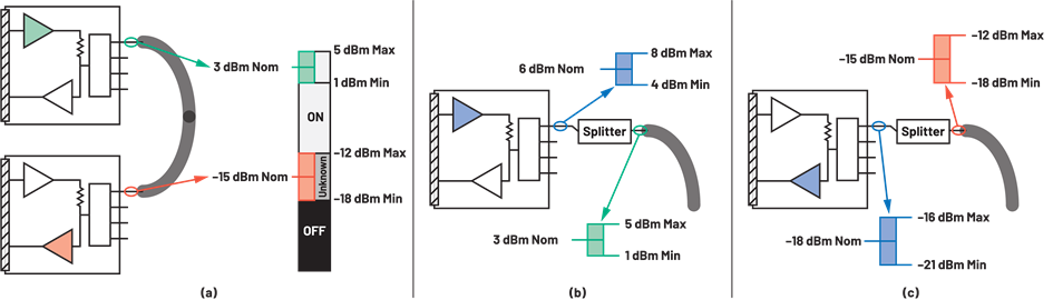
As with the older AISG designs, there was an inherent need to adjust the output level of the transmitter’s power amplifier (PA). This capability was helpful whenever a power splitter was used for circuits, such as the bypass channel shown in the v2.0 TMA example of Figure 1. Signal power adjustments were also useful if there was excessive attenuation in the 2.176 MHz band from RF filtering or lossy connections. The original modems provided this adjustability through the selection of external resistor values. These resistors were used to set the PA bias point and could be adjusted for the modem to meet the AISG signal requirements (see Figure 2a and 2b). Although there was some flexibility built into the v2.0 modems, the output power of the PA was essentially fixed at the design stage, because the only means to adjust the power required replacing the bias resistors.
Similar to the transmitter power drop, the receiver threshold could also be affected by a power splitter, in-line filtering, or other attenuation factors on the RF channel. Unfortunately, unlike the adjustable PA power, there was no adjustability of the ON/OFF threshold in any of the original v2.0 modems.
Power Saving Modes
Power savings are always high on a system designer’s list of requirements. Often, there is a power budget constraint applying pressure on more critical design elements, especially as the ALD hardware is scaled to more channels while being forced into an ever more compact footprint. Having some flexibility in less critical circuits (that is, the AISG modem) can give the designer more power budget for important blocks in the system.
One of the original AISG v2.0 modems on the market had a lower power standby mode, which would shut down the transmit circuitry to save a modest amount of power. Every milliamp helps, yet what would make for a better design is the ability to shut down not only the transmitter, but the receiver block and other unused portions of the modem itself. In opposition to additional power down features, the modem would need to be flexible enough to balance other use models, such as reference sharing.
Sharing a Reference Oscillator
Every AISG modem requires a reference signal to generate the 2.176 MHz carrier. This is typically provided with an 8.704 MHz crystal and an integrated oscillator circuit. All existing AISG modems on the market can be architected with a primary/secondary (or main/subordinate) circuit within the system, saving crystals, and thus reducing BOM costs.
Each chip can act as the primary crystal oscillator (XO) for downstream modems by buffering the signal through the SYNCOUT pin. This SYNCOUT signal is an open-drain output, which requires a simple external pull-up resistor to the analog supply so it can operate properly. This signal is then propagated to additional secondary modems downstream from the primary. The number of downstream modems is limited, but this reference sharing option is available.
Designing with this sharing architecture does have a drawback. Using any of the classic v2.0 modems, the primary would still need to burn as much power as any secondary modem. Thus, even though the system designer saves on components, there are no savings in their power budget.
Spectral Emissions
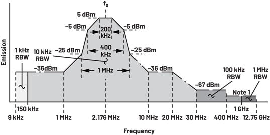
Finally, a primary requirement of the AISG standard for the PHY layer is the spectral purity of the modem’s transmitter. The spectral performance is delineated in AISG v3.0.0.3, section 10.3.11 – Modular Characteristics. Strict requirements limit the PA’s out-of-band spectral emissions, which tend to be very stringent. This is especially the case at the 30 MHz knee frequency where any harmonic noise must be below –67 dBm in absolute power, and where the resolution bandwidth (RBW) settings of the test instrumentation are the harshest. The PA output spectrum also must be balanced with the overall power level (that is, the adjustable transmit power), keeping within the absolute limits of the spectral mask. Increasing the PA power too much may cause a failure in the spectral mask.
Since there is no change to the emissions mask, integrated modems available for the v2.0 market also meet the v3.0 standards, although they often only provide a narrow 1 dB to ~4 dB of margin at the 30 MHz inflection point; thus, they limit the top end of the PA output power.
Using a v2.0 Modem in v3.0 System
All the features noted are available in a classic v2.0 modem. Since the PHY layer is essentially unchanged, each of the older modems meet the needs of an ALD system designer. Simply replicating existing AISG solutions detrimentally occupies more board space, impacts the system complexity, and may start to dominate the power budget, all while providing little to no improvement in performance and offering no feature upgrades. Fortunately, there is a new and improved alternative available for the AISG v3.0 market.
Upgraded Features Available in an AISG Modem
The first AISG v2.0 modem introduced to market included the original MAX9947. This device still provides a complete solution for interfacing between RS-485 and the defined 2.176 MHz OOK signal; thus, it remains fully compatible with the AISG v3.0 standard. Even though the original modem can service the standard, the expanded requirements in v3.0 provide an opportunity to enhance the existing design.
The MAX11947 comes with several performance improvements and added features to address many of the shortcomings inherent in using older generation ICs in a newer system. The primary feature in the modem is an integrated 4:1 multiplexer. This mux effectively provides four modems in one chip and facilitates automatic scanning. This gives the developer a tool to interact with for up to four RF ports while using nearly the same PCB footprint compared to an original modem. This integrated switching capability greatly reduces the need to specify and test additional circuits, such as RF switches, while reducing BOM requirements.
As shown in the earlier example, what was six modems in the AISG v2.0 system and potentially 16 modems required for a v3.0-capable system is now reduced to just five modems when incorporating the integrated 4:1 muxes (purple blocks in Figure 1). The modem/mux combination also provides a code free, non-microcontroller-based means to scan ports and identify a ping carrier signal with very little user intervention. The automatic port scanning feature helps to both map the hardware interconnects and find faults within the RF cabling system, completing the process with fewer IC components than is otherwise required.
An SPI interface not only controls the mux and modem but allows for the integration of features previously managed through external components. Parts like the PA power bias network (resistors) are now incorporated through a digitally adjustable transmit power. The modem also provides a new feature: an adjustable receive sensitivity threshold. Both adjustments help solve power splitting problems inherent in a bypass system, along with other inline attenuation issues. Not only can the transmit output be adjusted from about –0.5 dBm to about +7.0 dBm in 0.5 dB steps, but the modem can also independently adjust the receive comparison level as well. This allows the carrier detection threshold to range from about –15 dBm down to about –21.5 dBm. The adjustable transmit power and receive threshold can be modified on-the-fly, permitting the system designer to pass along this flexibility to the end user and allowing for improved system performance once installed in the field.
The device also incorporates several power modes: operational, standby, and power-down. This gives system designers many options to improve their power budget. The standby mode disables the transmitter circuitry like other classic modems from the v2.0 era, saving a typical 11 mA vs. the full operation mode. Even more savings are realized by disabling both the transmitter and the receiver circuitry with the power-down mode. This minimizes the power consumption (typically 20 mA lower than operation mode) while still allowing the modem to act as a primary oscillator for others downstream. If the SYNCOUT buffer is also shut down, the system designer can save over 23 mA vs. the operational mode.
This modem exceeds the spectral compliance of the previous generation modems, now giving the system designer about 15 dB of margin to the spectral mask at the 30 MHz point, thus allowing more flexibility on the transmitter power setting.
Finally, the device has a unique feature related to the serial interface: all the classic modem signals are mirrored within the SPI registers. This means additional GPIO, UART, or other port pins are not required on a microcontroller to interface with the modem signals. By reading from and writing to the mirrored bit, both interface and control can be exercised through the registers. The system designer now has the option to use the modem as a bridge between an RF port and an MCU with minimal resources.
Conclusion
The MAX11947 is built with purpose to meet the needs of the AISG v3.0 system designer. It provides added benefits and expands the role of the modem, while offering built-in flexibilities that go beyond just saving design time and BOM costs.


 combined with superior switching performance")


